TSMC Expects 5nm to be 11% of 2020 Wafer Production (sub 16nm)
by Dr. Ian Cutress on August 25, 2020 3:00 PM EST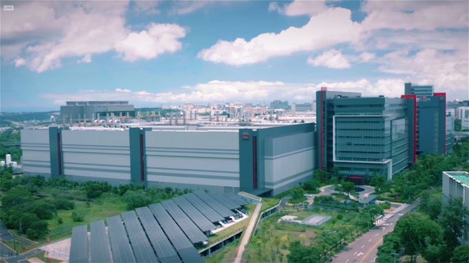
One of the measures of how quickly a new process node gains traction is by comparing how many wafers are in production, especially as that new process node goes through risk production and then into high volume manufacturing. You can tell a lot about how much confidence a foundry has in its new process by looking at the number of wafers in production, as well as the expected range of customers and products that are set to be produced. As part of TSMC’s Technology Symposium 2020, we were treated to a little insight into the growth of its new 5nm process technology.
TSMC’s 5nm process, or strictly speaking its first production version of 5nm, known as N5, is currently in the process of high volume manufacturing. We are expecting the first consumer products that use N5 processors, particularly smartphones, out by the end of the year. That means that the companies who are building those products have already worked with pre-production silicon for validation, put their orders in for N5 parts, and may already be getting the first deliveries of the new hardware.
With such a new process, we always expect that initial production, even in ‘high volume production’ mode, is usually slow. This is due to product development, but also extensive validation and to make sure that the product isn’t a dud (such as TSMC’s ill-fated 20nm process). However, judging by the slides produced by TSMC at its Technology Symposium, it looks like that 11% of its 2020 production of 16nm+ wafers will be on 5nm.
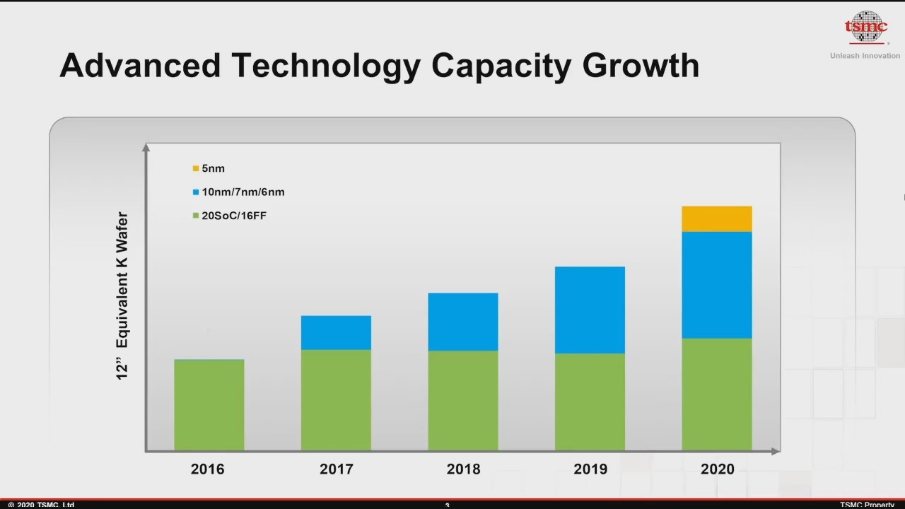
It should be noted that this graph has ’12-inch wafer equivalents’ as the y-axis, which means that if any process node would use 8-inch wafers, it would be scaled accordingly. However, all of these leading edge process nodes are likely to be on 12-inch wafers.
Unfortunately there’s no real sense of how many wafers that is. TSMC has stated in another slide that it produced over 12 million 12-inch wafer equivalents in 2019, but that covers all processes and all facilities. At financial disclosures, TSMC does a breakdown of each node, but only in terms of revenue.
However, comparing 5nm to TSMC’s 7nm capability, it does show that 2019 to 2020, 7nm increased by 22.7%, and in 2020, 5nm production will be ~24% of 7nm production. This leads into TSMC’s narrative that it expects to grow its 5nm production to double in 2021, and triple in 2022, using the 2020 numbers as a base.
TSMC did give some insight into its 5nm manufacturing facilities also.
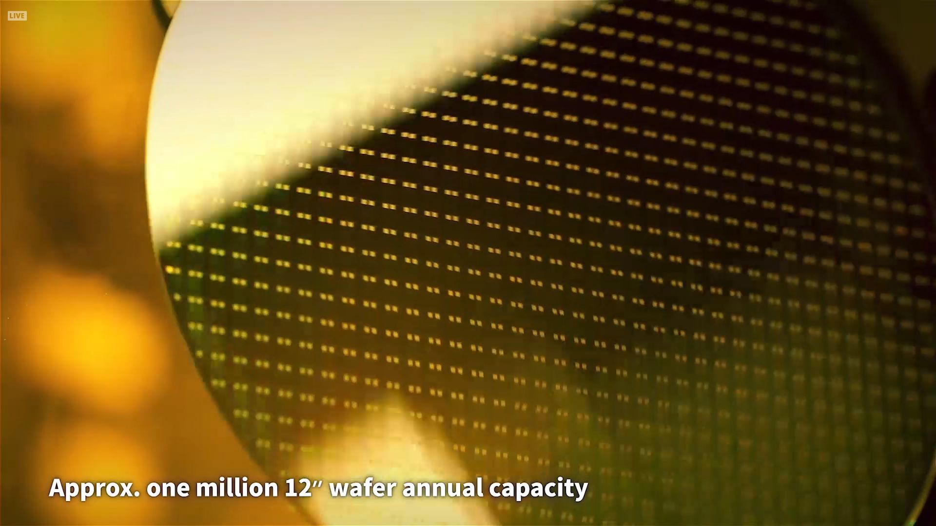
All of TSMC’s 5nm chips are being built at TSMC’s Fab 18, the newest fabrication plant that spreads over six buildings, which TSMC calls its ‘fourth GigaFab’. Fab 18 broke ground on January 26th 2018, and a year later the company started installing over 1300 manufacturing tools, including EUV machines, in a process that only took 8 months. From there, the company started testing its 5nm risk production, and started high-volume manufacturing in Q2. TSMC states that Fab 18 is capable of producing over one million 12-inch wafers per year, all on 5nm, and claims it leads the industry in energy efficiency for a fab of it size.
Related Reading
- TSMC Details 3nm Process Technology: Full Node Scaling for 2H22 Volume Production
- TSMC To Build 5nm Fab In Arizona, Set To Come Online In 2024
- TSMC & Broadcom Develop 1,700 mm2 CoWoS Interposer: 2X Larger Than Reticles
- TSMC Boosts CapEx by $1 Billion, Expects N5 Node to Be Major Success
- Early TSMC 5nm Test Chip Yields 80%, HVM Coming in H1 2020
- TSMC: 5nm on Track for Q2 2020 HVM, Will Ramp Faster Than 7nm
- TSMC: N7+ EUV Process Technology in High Volume, 6nm (N6) Coming Soon


13 Comments
View All Comments
dotjaz - Tuesday, August 25, 2020 - link
"However, all of these leading edge process nodes are likely to be on 12-inch wafers."Not "likely", they are on 12-inch wafers. There's no production 8-inch Fab in existence that can do 45nm and smaller, mainly because nobody bothered fitting 8-inch fabs with immersion lithography or multi-patterning. The most advanced 8-inch fab belongs to Samsung with 65/70nm nodes, everyone else stopped somewhere between 180nm-90nm.
albertmamama - Tuesday, August 25, 2020 - link
Maybe Dr. Cutress meant no 18-inch wafers?Yojimbo - Tuesday, August 25, 2020 - link
Where are there any 18 inch wafer fabs and who is making the equipment that goes into it?Ian Cutress - Wednesday, August 26, 2020 - link
It's more a comment towards development work, rather than production work. For example, if I recall correctly from my visit to Fab8, GF used 8-inch test workflow for 14nm several years before scale-up and production.Duncan Macdonald - Wednesday, August 26, 2020 - link
Very VERY fast construction - to get a huge fab from bare ground to full production in less than 2 years (and on a new process to boot) is impressive.(What a pity that government infrastructure projects can not manage the same speed - look at Crossrail in the UK or the Boston Big Dig in the US for really bad examples.)
smalM - Wednesday, September 2, 2020 - link
It was not from bare Ground.At the time of official ground breaking Dacin had already put a lot of work into that site.
But even considering that you are right, a very fast construction.
voiceofunreason - Monday, September 28, 2020 - link
Once-off/unique projects are always more expensive. Building a new fab is not that: it's repeating and iterating on an existing process.A better apples-apples comparison would be knowing ahead of time that you were going to build a third crossrail tunnel, and starting work on that just after finishing the first two. Or having an organisation that has a long term plan and funding to do nothing but tunnel expansions.
It still won't be China-speed but that's the cost of having property rights & input on government decisions, but I suspect you'll find that those government infrastructure projects wouldn't look so bad if they weren't always stop-start once-off projects.
psychobriggsy - Wednesday, August 26, 2020 - link
If Fab18 will eventually do around 90,000 wafers a month, and it's likely on the same scale as 7nm is currently, of which N5 is ~25%, then TSMC are probably making between 20,000 and 25,000 wafers a month on N5 (averaged over the year).But they only started half-way through the year, so perhaps Fab18 is 50% active already, at 40-50K wafers a month.
psychobriggsy - Wednesday, August 26, 2020 - link
But who is using this?Apple sell 200m iPhones a year. Let's call that 20m a month because some chips will go into iPads and AppleTVs. Assuming A14 is 100mm^2, then each wafer produced 500 working chips. 20m iPhones a month, that's 40000 wafers every month. Then there is A14X, and then MacAppleSilicon, and Huawei had a run earlier on before the ban, and maybe AMD/NVIDIA/Intel/Mediatek/etc also need a bit at the cherry.
psychobriggsy - Wednesday, August 26, 2020 - link
TBH A14 is probably 70mm^2 at most because of 5nm density, even if it has more cores and gpu and ai and cache...