Samsung Updates on GDDR6 Portfolio: 8 Gb and 16 Gb at Multiple Speeds
by Anton Shilov on January 25, 2018 12:01 PM EST
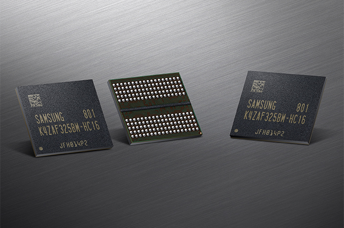
Samsung has issued an update to the GDDR6 announcement earlier this month. The company’s GDDR6 lineup will include chips featuring 8 Gb and 16 Gb capacities as well as speed bins not mentioned in the original announcement.
In addition to 16 Gb GDDR6 chips with 18 Gbps I/O speed, Samsung will offer GDDR6 with 12, 14 and 16 Gbps data transfer rates, thus targeting applications with different performance requirements. Also, two chip capacities (8 Gb and 16 Gb) will enable Samsung to target applications with various requirements for the amount of memory onboard.
Assuming both capacities will be made in all the speed bins, this gives the following:
| GPU Memory Math: Samsung GDDR6 | |||||||||
| 8 Gb (1 GB) | 16 Gb (2 GB) | ||||||||
| Bandwidth Per Pin (Gb/s) | 12 | 14 | 16 | 18 | 12 | 14 | 16 | 18 | |
| B/W per Chip/Stack (GB/s) | 48 | 56 | 64 | 72 | 48 | 56 | 64 | 72 | |
| Max Capacity | 256-bit | 8 GB | 16 GB | ||||||
| 384-bit | 12 GB | 24 GB | |||||||
| Total Bandwidth (GB/s) | 256-bit | 384 | 448 | 512 | 576 | 384 | 448 | 512 | 576 |
| 384-bit | 576 | 672 | 768 | 864 | 576 | 672 | 768 | 864 | |
Samsung’s 16 Gb GDDR6 chips could be used for various high-end products that benefit from large amounts of memory, including graphics cards and compute accelerators. By contrast, the company’s 8 Gb GDDR6 ICs will be handy for mainstream graphics cards that do not carry large amounts of memory.
Samsung did not announce pricing of its GDDR6 products, but it is logical to expect 16 Gb chips with an 18 Gbps data transfer rate to cost considerably more than 8 Gb ICs with lower speed bins. Therefore, the large portfolio will enable Samsung to capitalize on the new type of memory.
Related Reading
- Samsung Starts Mass Production of 16Gb GDDR6 Memory ICs with 18 Gbps I/O Speed
- Samsung Starts Production of 8 Gb DDR4-3600 ICs Using 2nd Gen 10nm-Class Tech
- Samsung Pre-Announces 16 Gbps GDDR6 Chips for Next-Gen Graphics Cards
- Micron Discusses GDDR: 16 Gbps GDDR5X, 16 nm GDDR6 and GDDR5
- SK Hynix Advances Graphics DRAM: GDDR6 Added to Catalogue, GDDR5 Gets Faster
Source: Samsung


19 Comments
View All Comments
haukionkannel - Thursday, January 25, 2018 - link
Hmmm. So 4-8 Gb with 128bit interface. Interesting to how much there will be those GPUs.limitedaccess - Thursday, January 25, 2018 - link
GDDR6 has the same clamshell mode support as GDDR5 and GDDR5x. Max capacity would technically be 32 GB for a 256 bit card and 48 GB for a 384 bit card with 2Gb dies.ImSpartacus - Thursday, January 25, 2018 - link
Have we seen that get used in any recent products?I think it's shown up in professional products historically, but I think it was a while ago.
mczak - Thursday, January 25, 2018 - link
I am quite sure this is still being used. The Quadro P5000 (gp104) and P6000 (gp102) have 256bit and 384bit memory interfaces, and to my knowledge only 8gb gddr5x chips are available. Those cards have 16GB and 24GB memory, respectively, twice that of the consumer parts, so it looks like they'd use clamshell mode.ImSpartacus - Thursday, January 25, 2018 - link
Yeah, that looks to be true. We only have 8Gb GDDR5X in production today, so that has to be clamshelled.limitedaccess - Friday, January 26, 2018 - link
It's typically only been used for professional due to the cost and to some extent the power. But some professional workloads can really make use of as much as possible and they can pay for it.The widest consumer usage of this for GDDR5 was actually the PS4 (they did switch to 8 1Gb dies eventually). On the GPU side the last time would have been the GTX 7xx series and respective Titan cards, maybe the 8GB 290/x versions as well.
willis936 - Thursday, January 25, 2018 - link
How large of an improvement is this really? In the past ten years we have seen capacity double a few times but have barely even seen a single doubling in throughput.dgingeri - Thursday, January 25, 2018 - link
That's what HBM is all about, but it is expensive. Using traces on a board has limitations. Most likely, we will see more and more multi-chip packages in the near future because of those limitations.Pork@III - Thursday, January 25, 2018 - link
What is number of limitations? More of 10 yeas ago has no problem to made boards for graphic cards with 512 bit wide bus between VRAM chips and GPU...Today 10+ years in future ''Houston, we have a problem''? Lies. lies!btmedic04 - Thursday, January 25, 2018 - link
its an issue with die sizes. a 512 bit bus needs a very large area of die space to interface into which increases difficulty in manufacturing and yields. can they do it today? sure, however its probably not economically feasible to the accountants to approve it