Apple’s A9 SoC Is Dual Sourced From Samsung & TSMC
by Ryan Smith on September 28, 2015 7:00 PM EST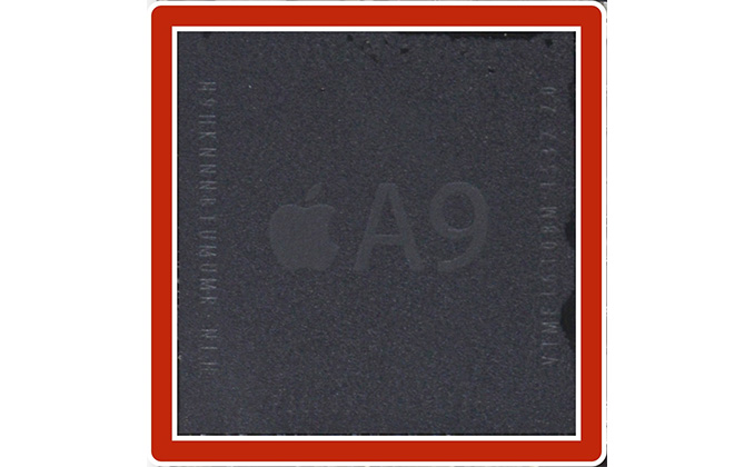
Picking up from our conversation this morning on Apple’s A9 SoC, the crew over at Chipworks has been working hard over the weekend to decap A9 and their first results are in. As it turns out, Chipworks has found chips fabbed by both TSMC and Samsung, which means that A9 is in fact a dual sourced part.
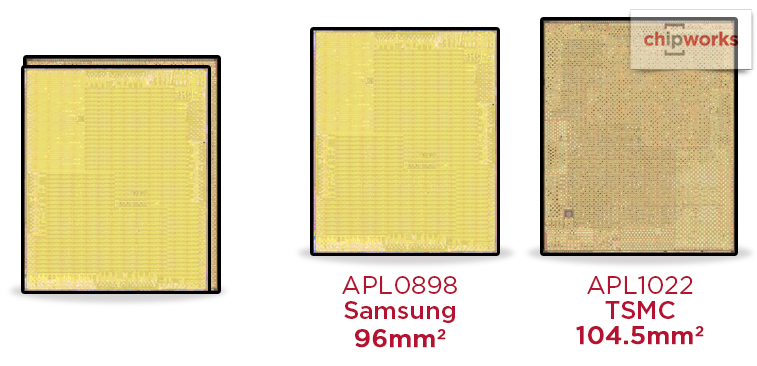
In taking apart iPhones and decapping SoCs, Chipworks has turned up two SoCs. The first, APL0898, is a 96mm2 A9 that’s fabbed by Samsung. The second SoC, APL1022, is a 104.5mm2 SoC fabbed by TSMC. And while Chipworks isn’t naming the specific manufacturing processes used, based on Apple’s comments on a “new transistor architecture,” we’re certainly looking at a form of FinFET. In which case the two chips are made on versions of Samsung’s 14nm FinFET and TSMC’s 16nm FinFET processes respectively.
This development is interesting for a few different reasons. From a fabrication standpoint, Samsung and TSMC have been brawling at multiple levels (technical and legal) to be the first to get a next-generation FinFET process out the door, with Samsung ultimately winning that battle when they shipped the 14nm Exynos 7420 for the Galaxy S6 family. For TSMC on the other hand this is as far as we know the first consumer product released with a 16nm TSMC fabbed part, indicating that TSMC is finally able to ship such parts in a reasonable volume.
More importantly, this is a huge move for Apple, and one we admittedly don’t have all of the facts about at this time. Dual sourcing parts is by no means a new concept – IBM requiring a second source of x86 chips is how AMD got started in the x86 industry, after all – but in more modern times dual sourcing of high performance parts is very rare due to how difficult and expensive it is. With dual sourcing essentially requiring the chip to be taped out twice – once for each fab – it requires significant financial and engineering resources, a cost that not very many companies besides Apple can take on without significant risk.
| Apple A9 SoC Versions | ||||
| APL0898 | APL1022 | |||
| Manufacturing Process | Samsung 14nm FinFET | TSMC 16nm FinFET | ||
| Die Size | 96mm2 | 104.5mm2 | ||
The big hurdle with dual sourcing a part such as a cutting-edge SoC like A9 is that unless the source fabs have designed their processes to be near identical – to form a common foundry specification – then different fabs will have different processes with different characteristics. This in turn is determined by the technical decisions a fab made in research and development, and the specific issues the fab ran into when bringing up the new process. The end result being that while two fabs can turn out chips based around the same design, those chips will not be identical. It’s this kind of inconsistency that chip customers like Apple have to tackle head-on if they want to go with dual sourcing.
Even at a physical level we can see this inconsistency right away in terms of die sizes. Despite the TSMC and Samsung processes being quite similar, the Samsung A9 is the smaller of the two by 8%, which as Chipworks notes is indicative of better density on Samsung’s 14nm node. What we don’t see, and the issue Apple really has to control for, is power consumption. Right now it’s a safe assumption that both chips can reach Apple’s required clockspeeds, so in order for Apple to utilize both in the iPhone 6s they need to make sure both perform as identically as possible, especially when it comes to idle power leakage and power consumption at different clockspeeds. The billion dollar question right now is whether either of the A9s is consistently better than the other one, and in which case by how much. For Apple it’s best that these chips are identical as possible – and they can make design choices when taping out the chip for each fab to help ensure this – but at the end of the day even Apple has to bow down to the laws of physics.
But the biggest unknown right now is why Apple would do this given the difficulties involved; to develop two A9s at twice the price. We can certainly speculate on reasons they would do this – yield issues at a fab, a desire to avoid putting all of their eggs in one basket and giving one fab too much power, or even just wanting to ramp up A9 production quickly by doubling the number of fabs working on it. But at the end of the day I don’t expect that’s a secret that will be known beyond the halls of One Infinite Loop, so speculation is all we have to work with for now.
In any case, if Apple has done their homework then dual sourcing A9s shouldn’t have an impact on average consumers, beyond perhaps ensuring that Apple has a sufficient supply to meet demand (ed: Apple sold 13mil iPhones in their opening weekend). Otherwise for techies, things are both more interesting and frustrating; just dual sourcing A9 makes an interesting product since this is something we almost never see done these days. As for the billion dollar question of which A9 is better, that will be a tossup. With enough time, effort, and a very large number of iPhones, it should be possible to coarsely determine if the A9s significantly differ in battery life, and thereby power consumption. However given the difficulties in taking an iPhone apart to access the A9, one would really need a software identification method to really make use of this information.
Source: Chipworks (A9 Shot Courtesy iFixit)


99 Comments
View All Comments
Soulkeeper - Monday, September 28, 2015 - link
This is good for competition.Rather than rewarding the fastest/first 100% they are spreading the money to keep them both fighting and prices down :) I can't wait to see these process techs hit x86, ddr4, gpu's, etc.
kwrzesien - Tuesday, September 29, 2015 - link
This is bad for GPU's, who would usually get the first crack at TSMC's newest process. Now we get stuck on 28nm forever. Apple is sucking up all the best capacity at TWO fabs now, not to mention a good bit at Intel too!astroboy888 - Saturday, October 3, 2015 - link
Don't worry about Nvidia and AMD GPUs, TSMC has plenty of capacity for their 16FF+ line. Counting all of the Apple A9s won't exceed 2% of TSMC's total capacity.The Pascal/Fiji GPUs will be delivered on time and the gamer's will rejoice.
Just42 - Monday, September 28, 2015 - link
Its not all of that hard to dual source as long as you keep the analog delta to a minimum. The tools do a lot of work once you get the timing files from the vendors and your internal tools group and follow good layout rules . Plus the cost of the mask set (4-7million or so) is what ,maybe 2 minutes of sales for Apple. This is nothing compared to if one of these vendors have an excursion.Someone, please put a decent graphing power meter on VccMain and run the benchmarks and see what the delta is.
Vishalaestro - Monday, September 28, 2015 - link
Why can't Apple USE Intel for surfing the chips ,they have a far better chips compared to Samsung or tsmc.Vishalaestro - Monday, September 28, 2015 - link
Edit:Intel,as far as I know has the world best process node so u still dont find a reason why Apple is not using Intel fabWorldWithoutMadness - Tuesday, September 29, 2015 - link
Every stumbled upon the term 'money'?astroboy888 - Tuesday, September 29, 2015 - link
The reasons are too long to get into. It has a lot to do with legacy. Every fabless semiconductor company uses TSMC's design rules over 30 years. In a way, the entire chip design industry standardized on TSMC's rules, spice models, tool sets, and reference flows.Many reason why transitioning to Intel is difficult. 1) software retooling takes about 2-3 years. you have to stay in bed with Intel for 2 years even to get your first product out. Do you trust them? 2. Intel being a secretive and paranoid companies often don't want to share what they consider as proprietary secrets. This makes specialized design tweaking very difficult. Apple does a lot of this to push the process to the limit. 3. Intel potentially become a "frienemie" - both a supplier and competitor. Question is when Intel is short of manufacturing capacity for their CPU, do they focus on their own production first or honor their contract to Apple? For these reasons, Apple prefers to work with the likes of TSMC - "pure-play" foundry. This way there is no conflict of interest.
Michael Bay - Tuesday, September 29, 2015 - link
>guarding trade secrets>secretive and paranoid
baconforall - Monday, September 28, 2015 - link
Something to note here is that tsmc is using their old back end of line metallization from their 20soc process. This is the limiting factor for the chip size. The reported transistor gate length of 16 or 14 nm makes no difference.