Intel’s ‘Tick-Tock’ Seemingly Dead, Becomes ‘Process-Architecture-Optimization’
by Ian Cutress on March 22, 2016 6:45 PM EST
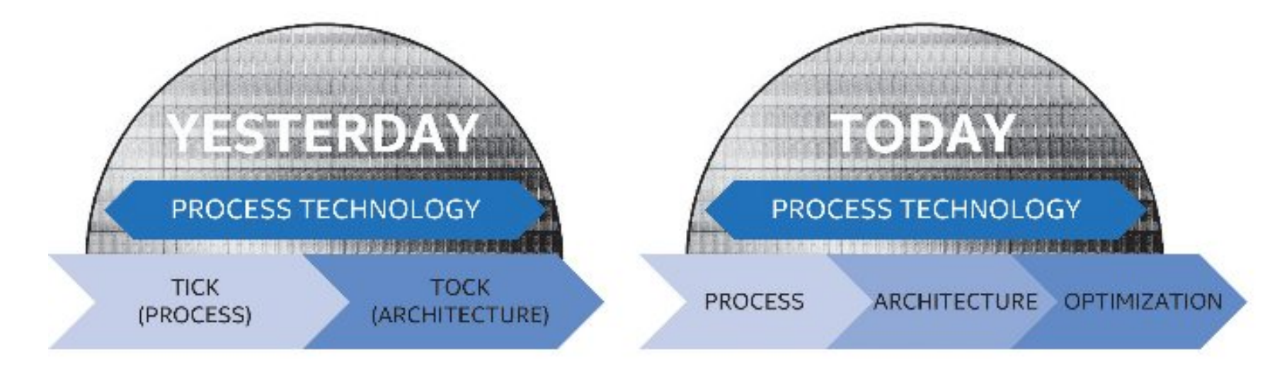
As reported at The Motley Fool, Intel’s latest 10-K / annual report filing would seem to suggest that the ‘Tick-Tock’ strategy of introducing a new lithographic process note in one product cycle (a ‘tick’) and then an upgraded microarchitecture the next product cycle (a ‘tock’) is going to fall by the wayside for the next two lithographic nodes at a minimum, to be replaced with a three element cycle known as ‘Process-Architecture-Optimization’.
Intel’s Tick-Tock strategy has been the bedrock of their microprocessor dominance of the last decade. Throughout the tenure, every other year Intel would upgrade their fabrication plants to be able to produce processors with a smaller feature set, improving die area, power consumption, and slight optimizations of the microarchitecture, and in the years between the upgrades would launch a new set of processors based on a wholly new (sometimes paradigm shifting) microarchitecture for large performance upgrades. However, due to the difficulty of implementing a ‘tick’, the ever decreasing process node size and complexity therein, as reported previously with 14nm and the introduction of Kaby Lake, Intel’s latest filing would suggest that 10nm will follow a similar pattern as 14nm by introducing a third stage to the cadence.
From Intel's report: As part of our R&D efforts, we plan to introduce a new Intel Core microarchitecture for desktops, notebooks (including Ultrabook devices and 2 in 1 systems), and Intel Xeon processors on a regular cadence. We expect to lengthen the amount of time we will utilize our 14nm and our next generation 10nm process technologies, further optimizing our products and process technologies while meeting the yearly market cadence for product introductions.
While the new PAO or ‘Process-Architecture-Optimization’ model is a direct result of the complexity of developing and implementing new lithographic nodes (Intel has even entered into a new five-year agreement with ASML to develop new extreme-ultra-violet lithographic techniques), but also with new process nodes typically comes a time where yields have to become high enough to remain financially viable in the long term. It has been well documented that the complexity of Intel’s 14nm node using the latest generation FinFET technology took longer than expected to reach maturation point compared to 22nm. As a result, product launches were stretched out and within a three-year cycle Intel was starting to produce only two new generations of products.
Intel’s current fabs in Ireland, Arizona, and Oregon are currently producing wafers on the 14nm node, with Israel joining Arizona and Oregon on the 22nm node. Intel also has agreements in place for third-party companies (such as Rockchip) to manufacture Intel’s parts for certain regional activity. As well as looking forward to 10nm, Intel’s filing also states projects in the work to move from 300mm wafers to 450mm wafers, reducing cost, although does not put a time frame on it.
The manufacturing lead Intel has had over the past few years over rivals such as Samsung, TSMC and Global Foundries, has put them in a commanding position in both home computing and enterprise. One could argue that by elongating the next two process nodes, Intel might lose ground on their advantage, especially as other companies start hitting their stride. However, the research gap is still there - Intel introduced 14nm back in August 2014, and has since released parts upwards of 400mm2, whereas Samsung 14nm / TSMC 16nm had to wait until the launch of the iPhone to see 100mm2 parts on the shelves, with Global Foundries still to launch their 14nm parts into products. While this relates to density, both power and performance are still considered to be on Intel’s side, especially for larger dies.
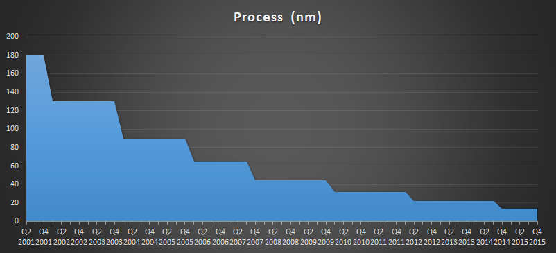
Intel's Current Process Over Time
On the product side of things, Intel’s strategy of keeping the same microarchitecture for two generations allows its business customers to guarantee the lifetime of the halo platform, and maintain consistency with CPU sockets in both consumer and enterprise. Moving to a three stage cycle has thrown some uncertainty on this, depending on how much ‘optimization’ will go into the PAO stage: whether it will be microarchitectural, better voltage and thermal qualities, or if it will be graphics focused, or even if it will keep the same socket/chipset. This has a knock on effect with Intel’s motherboard partners, who have used the updated socket and chipset strategy every two generations as a spike in revenue.
Suggested Reading:
EUV Lithography Makes Good Progress, Still Not Ready for Prime Time
Tick Tock on the Rocks: Intel Delays 10nm, adds 3rd Gen 14nm
The Intel Skylake Mobile and Desktop Launch with Microarchitecture Analysis
Source: Intel 10-K (via The Motley Fool)


98 Comments
View All Comments
JoeyJoJo123 - Wednesday, March 23, 2016 - link
Increases in what? Performance or transistor count?Because Moore's law does not say anything about the performance doubling every 18 months, only that the amount of transistors that can be placed on the same size chip can be doubled every 18 months and cost about the same. Doubling the amount of transistors does not mean doubling the performance. It just means that it doubles the complexity of manufacturing that chip.
If you're one of the sorry few that misunderstands Moore's law to be about performance gains, then you truly have my condolences.
extide - Thursday, March 24, 2016 - link
Moore's law is doubling the number of transistors every 18-24 months. Not throughput.cobrax5 - Wednesday, March 23, 2016 - link
You can't possibly think GPU's have stagnated, can you? Forget that they've been on 28nm for freaking ever, GPU's are highly parallel, and therefore can have more transistors thrown at increasing performance. The most recent gen GPU's are often > 50% faster than the previous gen, that's a whole lot better than the 5-15% you get with CPU's, especially since CPU's are still highly dependant on single threaded performance.zodiacfml - Wednesday, March 23, 2016 - link
This is simply Intel telling everyone that there's not much competitionMeteor2 - Wednesday, March 23, 2016 - link
Intel compete with themselves. They want people to buy new chips. They don't want people to buy one chip then use it forever.Looks like 10 nm in 2017, 7 nm in 2020-21, and 5 nm in mid-2020s.
name99 - Wednesday, March 23, 2016 - link
Perhaps Intel should have though of that before randomly spraying new features across each new processor generation in such an incoherent fashion that no-one actually bothers to support them because chances are their customers won't have the right chip to utilize the feature.*cough* TSX *cough* various flavors of AVX *cough* SHA *cough* ...
trane - Wednesday, March 23, 2016 - link
The tick-tock was never a yearly cycle. It was always more like 1 year and 2-3 months per tick or tock. The first tick was in January. By Broadwell, that had slipped to December, one full year behind the tick-tock schedule. Now with three generations per process, they might actually accelerate generations from 1 year 2/3 months to 1 year.naveenarur - Wednesday, March 23, 2016 - link
Hickory-Dickory-DockPork@III - Wednesday, March 23, 2016 - link
Tick Tock lie than come another lie. Capitalism.cobrax5 - Wednesday, March 23, 2016 - link
Yeah, like all those awesome CPU's produced by communist economies...hah...