TSMC
Taiwan Semiconductor Manufacturing Co. this week said its revenue for the second quarter 2024 reached $20.82 billion, making it the company's best quarter (at least in dollars) to date. TSMC's high-performance computing (HPC) platform revenue share exceeded 52% for the first time in many years due to demand for AI processors and rebound of the PC market. TSMC earned $20.82 billion USD in revenue for the second quarter of 2024, a 32.8% year-over-year increase and a 10.3% increase from the previous quarter. Perhaps more remarkable, $20.82 billion is a higher result than the company posted Q3 2022 ($20.23 billion), the foundry's best quarter to date. Otherwise, in terms of profitability, TSMC booked $7.59 billion in net income for the quarter, for a gross margin of...
Hot Chips 31 Keynote Day 2: Dr. Phillip Wong, VP Research at TSMC (1:45pm PT)
The keynote for the second day is from TSMC, with Dr. Phillip Wong taking the stage to talk about the latest developments in TSMC's research and portfolio. The talk...
12 by Dr. Ian Cutress on 8/20/2019
Hot Chips 31 Live Blogs: Intel Spring Crest NNP-T on 16nm TSMC
Intel is showing us some of the design features of its new ML training product, Spring Crest.
4 by Dr. Ian Cutress on 8/19/2019
TSMC Announces Performance-Enhanced 7nm & 5nm Process Technologies
TSMC has quietly introduced a performance-enhanced version of its 7 nm DUV (N7) and 5 nm EUV (N5) manufacturing process. The company’s N7P and N5P technologies are designed for...
36 by Anton Shilov on 7/30/2019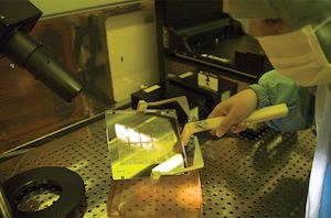
TSMC: 3nm EUV Development Progress Going Well, Early Customers Engaged
Development of new fabrication technologies never stops at leading-edge companies such as TSMC. Therefore, it is not surprising to hear the annoucement that development of TSMC’s 3nm node is...
76 by Anton Shilov on 7/23/2019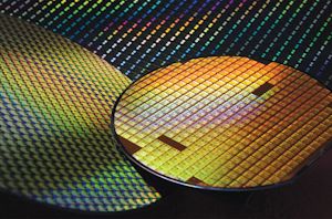
TSMC: Most 7nm Clients Will Transition to 6nm
In this week's quarterly earnings conference call, TSMC’s revealed that the company expects most of its 7nm "N7" process customers to eventually transition to its forthcoming 6nm "N6" manufacturing...
39 by Anton Shilov on 5/1/2019
TSMC: No Plans to Buy Rivals at The Moment
Although TSMC expects demand for chips to increase going forward and despite an ongoing trend towards consolidation on the foundry market, the company has commented that it currently has...
4 by Anton Shilov on 4/22/2019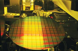
TSMC Reveals 6 nm Process Technology: 7 nm with Higher Transistor Density
TSMC this week unveiled its new 6 nm (CLN6FF, N6) manufacturing technology, which is set to deliver a considerably higher transistor density when compared to the company's 7 nm...
23 by Anton Shilov on 4/17/2019
TSMC’s 5nm EUV Making Progress: PDK, DRM, EDA Tools, 3rd Party IP Ready
TSMC this week has said that it has completed development of tools required for design of SoCs that are made using its 5 nm (CLN5FF, N5) fabrication technology. The...
33 by Anton Shilov on 4/5/2019
TSMC’s Fab 14B Photoresist Material Incident: $550 Million in Lost Revenue
TSMC on Friday revealed more details regarding an incident with a photoresist material at its Fab 14B earlier this year. The contaminated chemical damaged wafers on TSMC’s 12 nm...
29 by Anton Shilov on 2/20/2019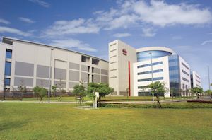
TSMC Chip Yields Hit By Bad Chemical Batch
TSMC on Monday said that some of the wafers it has processed recently have lower yields because of a chemical it uses during production. The company began investigation and...
28 by Anton Shilov on 1/29/2019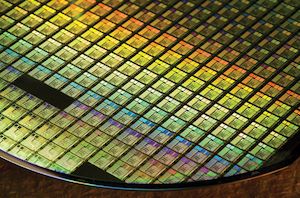
ASML to Ship 30 EUV Scanners in 2019: Faster EUV Tools Coming
ASML said last week that it planned to ship 30 extreme ultraviolet scanners in 2019, up significantly from 2018. The plan is not surprising, as demand for EUV lithography...
17 by Anton Shilov on 1/28/2019
TSMC: 7nm Now Biggest Share of Revenue
As process node technology gets ever more complex, it costs big dollars to develop and then building chips on the process is also a very costly process. The big...
44 by Ian Cutress on 1/17/2019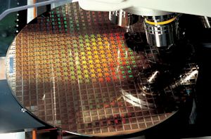
TSMC: First 7nm EUV Chips Taped Out, 5nm Risk Production in Q2 2019
Last week, TSMC made two important announcements concerning its progress with extreme ultraviolet lithography (EUVL). First up, the company has successfully taped out its first customer chip using its...
50 by Anton Shilov on 10/9/2018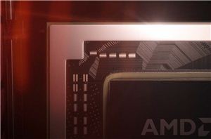
AMD's 7nm CPUs & GPUs To Be Fabbed by TSMC, on Track for 2018 - 2019
With the announcement that its long-time manufacturing partner (and outright former fab) GlobalFoundries is dropping out of the race for bleeding-edge manufacturing nodes, the second big question of the...
28 by Ryan Smith & Anton Shilov on 8/27/2018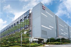
TSMC: Outbreak of Malware That Triggered Delays & Losses Caused by Software for New Tool
TSMC announced this week that it suffered a computer malware outbreak, resulting in a roughly 3 day outage for parts of the fab while systems were restored. As a...
42 by Anton Shilov on 8/9/2018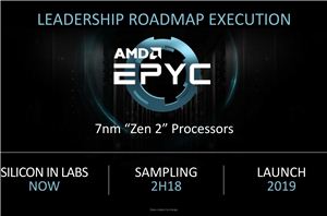
AMD “Rome” EPYC CPUs to Be Fabbed By TSMC
Along with AMD’s epic quarterly results that were announced yesterday afternoon, there was also an interesting nugget buried in the earnings call for the results. We’ve known for some...
32 by Ryan Smith on 7/26/2018
TSMC Details 5 nm Process Tech: Aggressive Scaling, But Thin Power and Performance Gains
At a special event last week, TSMC announced the first details about its 5 nm manufacturing technology that it plans to use sometime in 2020. CLN5 will be the...
10 by Anton Shilov on 5/8/2018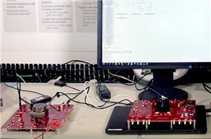
Cadence and Micron Demo DDR5-4400 IMC and Memory, Due in 2019
Cadence this week introduced the industry’s first IP interface in silicon for the current provisional DDR5 specification developed by JEDEC. Cadence’s IP and test chip us fabricated using TSMC’s...
31 by Anton Shilov on 5/3/2018
TSMC Kicks Off Volume Production of 7nm Chips
TSMC last week announced that it had started high volume production (HVM) of chips using their first-gen 7 nm (CLN7FF) process technology. The contract maker of semiconductors says it...
63 by Anton Shilov on 4/24/2018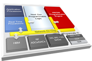
Xilinx Announces Project Everest: The 7nm FPGA SoC Hybrid
This week Xilinx is making public its latest internal project for the next era of specialized computing. The new product line, called Project Everest in the interim, is based...
16 by Ian Cutress on 3/19/2018


