TSMC
Taiwan Semiconductor Manufacturing Co. this week said its revenue for the second quarter 2024 reached $20.82 billion, making it the company's best quarter (at least in dollars) to date. TSMC's high-performance computing (HPC) platform revenue share exceeded 52% for the first time in many years due to demand for AI processors and rebound of the PC market. TSMC earned $20.82 billion USD in revenue for the second quarter of 2024, a 32.8% year-over-year increase and a 10.3% increase from the previous quarter. Perhaps more remarkable, $20.82 billion is a higher result than the company posted Q3 2022 ($20.23 billion), the foundry's best quarter to date. Otherwise, in terms of profitability, TSMC booked $7.59 billion in net income for the quarter, for a gross margin of...
ASML High-NA Development Update: Coming to Fabs in 2024 - 2025
It took the semiconductor industry over a decade to prep everything needed for production of chips using extreme ultraviolet (EUV) lithography. It looks like it is going to take...
8 by Anton Shilov on 5/26/2022
TSMC Roadmap Update: N3E in 2024, N2 in 2026, Major Changes Incoming
Taiwan Semiconductor Manufacturing Co. has solid plans for the next few years, but the foundry's manufacturing technology design cycles are getting longer. As a result, to address all of...
21 by Anton Shilov on 4/22/2022Universal Chiplet Interconnect Express (UCIe) Announced: Setting Standards For The Chiplet Ecosystem
If there has been one prominent, industry-wide trend in chip design over the past half-decade or so, it has been the growing use of chiplets. The tiny dies have...
25 by Ryan Smith on 3/2/2022
AMD: We’re Using an Optimized TSMC 5nm Process
When AMD started using TSMC’s 7nm process for the Zen 2 processor family that launched in November 2019, one of the overriding messages of that launch was that it...
44 by Dr. Ian Cutress on 1/10/2022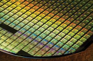
TSMC Unveils N4X Node: Extreme High-Performance at High Voltages
TSMC this week announced a new fabrication process that is tailored specifically for high-performance computing (HPC) products. N4X promises to combine transistor density and design rules of TSMC's N5-family...
42 by Anton Shilov on 12/17/2021
Semi CapEx to Hit $152 Billion in 2021 as Market on Track for $2 Trillion by 2035
Semiconductor makers have drastically increased their capital expenditures (CapEx) this year in response to unprecedented demand for chips that is going to last for years. Now the CEO of...
8 by Anton Shilov on 12/17/2021
AMD Gives Details on EPYC Zen4: Genoa and Bergamo, up to 96 and 128 Cores
Since AMD’s relaunch into high-performance x86 processor design, one of the fundamental targets for the company was to be a competitive force in the data center. By having a...
36 by Dr. Ian Cutress on 11/8/2021
TSMC Roadmap Update: 3nm in Q1 2023, 3nm Enhanced in 2024, 2nm in 2025
TSMC has introduced a brand-new manufacturing technology roughly every two years over the past decade. Yet as the complexity of developing new fabrication processes is compounding, it is getting...
32 by Anton Shilov on 10/18/2021
TSMC to Build Japan's Most Advanced Semiconductor Fab
Fabs are well-known for being an expensive business to be in, so any time a new fab is slated for construction, it tends to be a big deal &ndash...
14 by Anton Shilov on 10/15/2021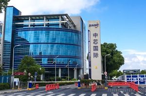
China's SMIC To Build a GigaFab for $8.87B: An Answer to the Shortages
As a result of being on the US Entity list, SMIC's blacklisting has caused troubles in the company developing and deploying leading-edge fabrication technologies. As a result, it has...
23 by Anton Shilov on 9/6/2021-page-036a_carousel.jpg)
Xilinx Expands Versal AI to the Edge: Helping Solve the Silicon Shortage
Today Xilinx is announcing an expansion to its Versal family, focused specifically on low power and edge devices. Xilinx Versal is the productization of a combination of many different...
25 by Dr. Ian Cutress on 6/9/2021
An AnandTech Interview with TSMC: Dr. Kevin Zhang and Dr. Maria Marced
In the past week, TSMC ran its 2021 Technology Symposium, covering its latest developments in process node technology designed to improve the performance, costs, and capabilities for its customers...
18 by Dr. Ian Cutress on 6/8/2021
TSMC Manufacturing Update: N6 to Match N7 Output by EOY, N5 Ramping Faster, Better Yields Than N7
As part of a regular TSMC Technology Symposium, the foundry published updates on its status on it’s current leading-edge manufacturing technologies, the N7, N5 and their respective derivatives such...
50 by Andrei Frumusanu on 6/1/2021
AMD Demonstrates Stacked 3D V-Cache Technology: 192 MB at 2 TB/sec
The AMD team surprised us here. What seemed like a very par-for-the-course Computex keynote turned into an incredible demonstration of what AMD is testing in the lab with TSMC’s...
93 by Dr. Ian Cutress on 5/31/2021
AMD Ryzen 5000G: Zen 3 APUs for Desktop Coming August 5th
Back in April of this year, AMD announced its new series of Ryzen 5000G processors with integrated graphics. These processors were an upgrade over the previous generation of 4000G...
35 by Dr. Ian Cutress on 5/31/2021
TSMC Update: 2nm in Development, 3nm and 4nm on Track for 2022
For TSMC, being the world's largest foundry with nearly 500 customers has its peculiarities. On the one hand, the company can serve almost any client with almost any requirements...
74 by Anton Shilov on 4/26/2021
Sales of Fab Tools Surge to Over $71 Billion in 2020
SEMI, an organization representing chipmakers and producers of semiconductor production tools, published this week that sales of wafer processing equipment has surged to an all-time record of $71.19 billion...
18 by Anton Shilov on 4/15/2021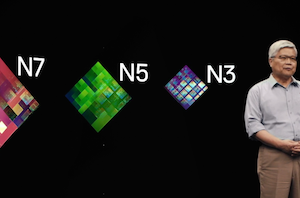
TSMC Q1 2021 Process Node Revenue: More 7nm, No More 20nm
This week TSMC has disclosed its full quarterly financial results for Q1 2021. In those results the company often explains where the revenue demand is for its technologies, and...
40 by Dr. Ian Cutress on 4/15/2021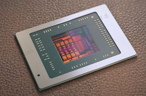
AMD Ryzen 5000G APUs: OEM Only For Now, Full Release Later This Year
With the high demand for semiconductors causing most companies to focus on their high margin, high profitability components, I wasn’t expecting to see many launches of low-to-mid range hardware...
67 by Dr. Ian Cutress on 4/13/2021
TSMC to Spend $100B on Fabs and R&D Over Next Three Years: 2nm, Arizona Fab & More
TSMC this week has announced plans to spend $100 billion on new production facilities as well as R&D over the next three years. The world's largest contract maker of...
45 by Anton Shilov on 4/2/2021


