The Qualcomm Snapdragon 820 Performance Preview: Meet Kryo
by Ryan Smith & Andrei Frumusanu on December 10, 2015 11:00 AM EST- Posted in
- SoCs
- Snapdragon
- Qualcomm
- Snapdragon 820

I don’t think there’s any way to sugarcoat this, but 2015 has not been a particularly great year for Qualcomm in the high-end SoC business. The company remains a leading SoC developer, but Snapdragon 810, the company’s first ARMv8 AArch64-capable SoC, did not live up to expectations. Seemingly held back by design matters and a rough 20nm planar manufacturing process – a problem shared by many vendors in the last year – Snapdragon 810 couldn’t make good use of its highly clocked ARM Cortex-A57 cores, and ultimately struggled in the face of SoCs built on better processes such as Samsung’s surprisingly early Exynos 7420.
But the purpose of today’s article isn’t to reminisce about the past, rather it’s to look towards the future. Qualcomm knows all too well what has happened in the past year and the cost to the company that has come from it, so now they need to dust themselves off and try again. With Samsung’s more advanced 14nm FinFET process in hand, a new CPU core, a new GPU, and a number of other advancements, Qualcomm is ready to try again; to try to recapture the good old days of 28nm and their Krait CPU architecture.
To that end Qualcomm started talking about Snapdragon 820 early and doing so loudly. Last month the company held their first press demonstration of the SoC, showcasing early demonstrations in action and going into more detail than ever before on their performance and power projections for their next-generation SoC.
If there is any unfortunate aspect to any of this, it’s that while Qualcomm is showing off Snapdragon 820 today, it won’t be ready for the holidays (lining up with what we expect will be the typical spring smartphone refreshes). But some of this is clearly driven by Qualcomm’s business needs and the aforementioned effort at Qualcomm to quickly pick themselves up and try again.
Meanwhile after last month’s demonstrations, this month Qualcomm is ready to move on to the next phase in what has become their traditional roll-out process for a new SoC: giving the press access to the company’s Mobile Development Platform (MDP) devices. Designed for software developers to begin building apps and (for lack of a better word) experiences around the new SoC, the MDP is something of the home-stretch in SoC development, as it means Qualcomm is ready to let the press and developers see the hardware and near-final software stack. We’ve previously previewed the Snapdragon 800, 805, and 810 via their MDPs, and for Snapdragon 820 Qualcomm has once again opted to do the same. So without further ado, let’s take our first look at Snapdragon 820.
| Qualcomm Snapdragon S810 Specifications | |||
| SoC | Snapdragon 820 | Snapdragon 810 | Snapdragon 800 |
| CPU | 2x Kryo@1.593GHz 512KB(?) L2 cache 2x Kryo@2.150GHz 1MB(?) L2 cache |
4x A53@1.555GHz 512KB L2 cache 4x A57@1.958GHz 2MB L2 cache |
4x Krait 400@2.45GHz 4x512KB L2 cache |
| Memory Controller |
2x 32-bit LPDDR4 @ 1803MHz 28.8GB/s b/w |
2x 32-bit LPDDR4 @ 1555MHz 24.8GB/s b/w |
2x 32-bit LPDDR3 @ 933MHz 14.9GB/s b/w |
| GPU | Adreno 530 @ 624MHz |
Adreno 430 @ 600MHz |
Adreno 330 @ 600MHz |
| Mfc. Process |
Samsung 14nm LPP |
TSMC 20nm SoC |
TSMC 28nm HPm |
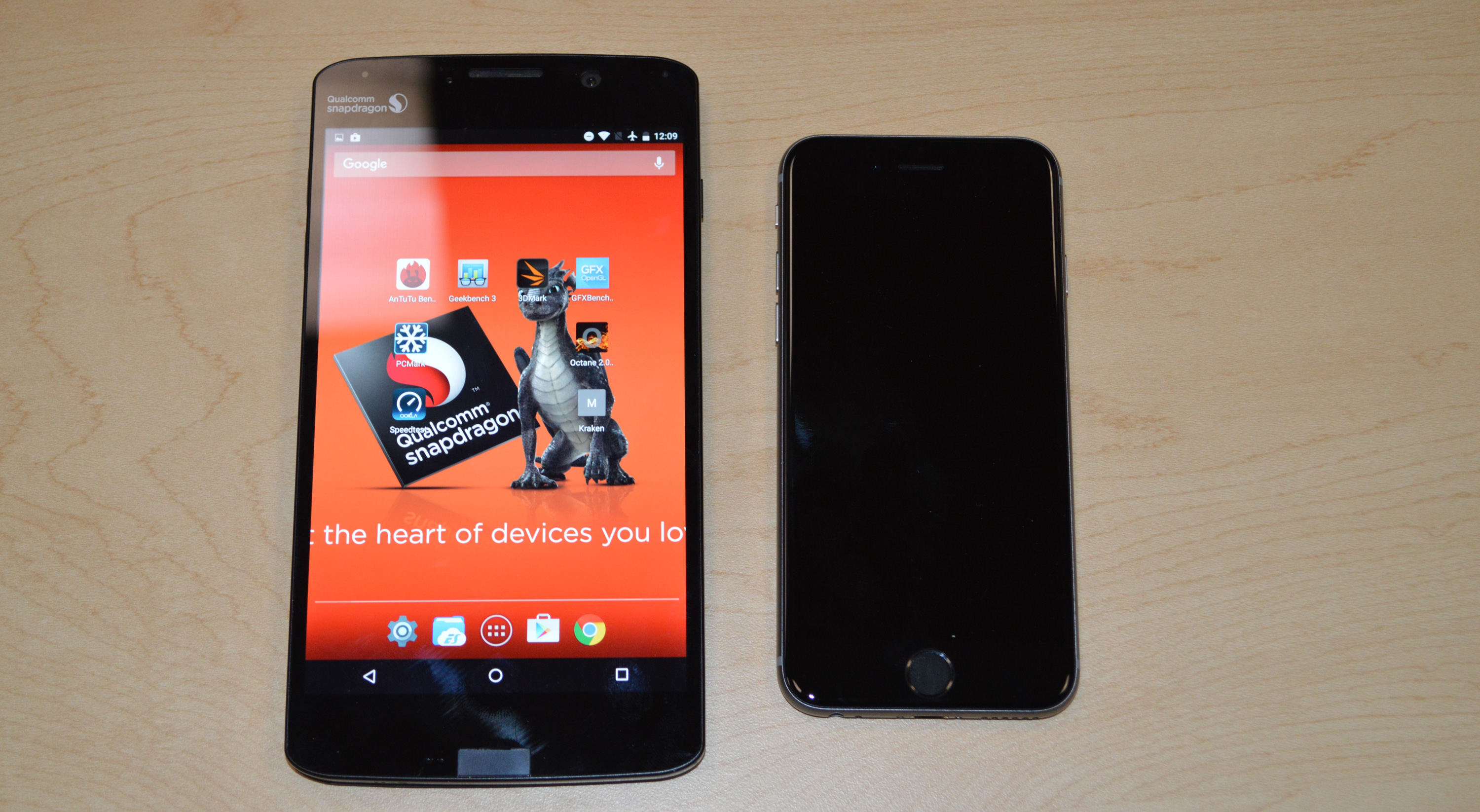
Taking a trek down to sunny San Diego, Qualcomm handed to us the Snapdragon 820 MDP/S. A 6.2” phablet, the MDP/S is a development kit designed for function over form, containing a full system implementation (sans cellular) in an otherwise utilitarian design. Along with the Snapdragon 820 SoC, the 820 MDP/S also includes a 6.2” 2560x1600 display, 3GB of LPDDR4 memory runnning at a slightly higher 1804MHz instead of 1555MHz we've seen on the Snapdragon 810 and Exynos 7420, a 64GB Universal Flash Storage package, a 21MP rear camera, 802.11ac WiFi, and a Sense ID ultrasonic fingerprint scanner. Overall the aesthetics of the MDP/S differs significantly from what retail phones will go for, but internally the MDP/S won’t be far removed from the kinds of configurations we’ll see in 2016 smartphones.
Overall there’s little to report on the MDP/S experience itself. Qualcomm is still sorting out some driver bugs – only one device in our group was ready to run PCMark – and to be sure like past Qualcomm MDP previews this is very much a preview. However the experience was otherwise unremarkable (in a good way) with our unit completing all of our tests bar part of SPEC CPU 2000, which will require further analysis.
More interesting from a testing perspective is that Qualcomm opted to demonstrate Snapdragon 820 using the MDP/S smartphone development kit, instead of a larger MDP/T tablet development kit. Qualcomm has used MDP/T for the press demonstrations on both Snapdragon 800 and Snapdragon 810, so the fact that they are once again using the MDP/S is very notable. From a pure performance perspective the MDP/T allowed Qualcomm to show off previous Snapdragon designs at their best – these are just performance previews, after all – but after Snapdragon 810 I don’t doubt that had this been another MDP/T that the 820’s thermals and power consumption would be called into question. So instead we are looking at 820 in a phablet, and while this may not put 820 in the best possible light, the end result is that we get to see what performance in a large phone looks like, and for Qualcomm there isn’t any doubt about 820’s suitability for a smartphone.
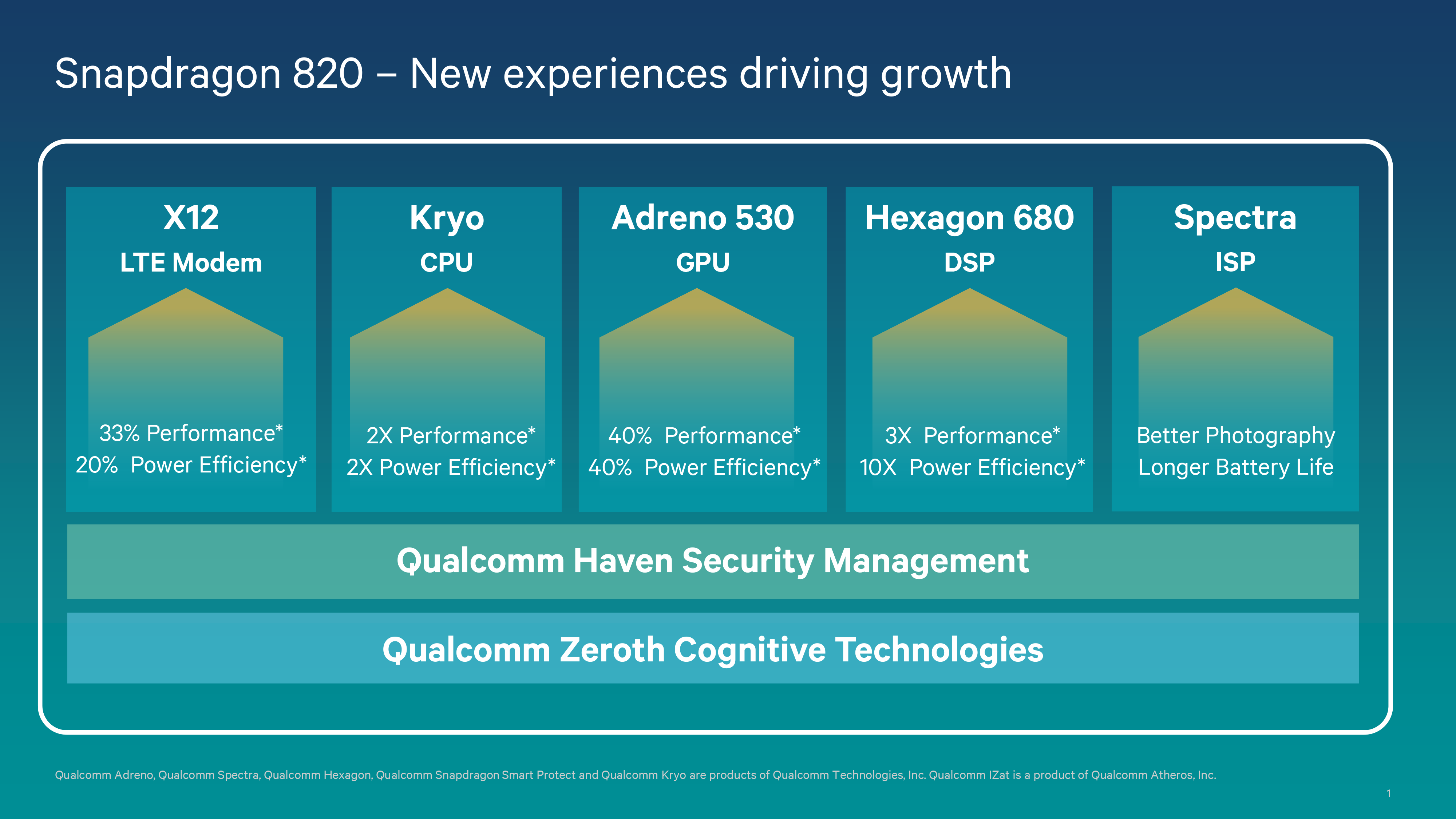
As for Snapdragon 820 itself, we’ve already covered the SoC in some depth in past articles – and this week’s preview doesn’t come with much in the way of new architectural information – but here’s a quick recap of what we know so far. 820 uses a new Qualcomm developed CPU core called Kryo. The quad core CPU is best described as an HMP solution with two high-performance cores clocked at 2150 MHz and two low-power cores clocked at 1593MHz. The CPU architectures of both clusters are identical, but with differences in cache configuration and their power/frequency tuning.
Meanwhile the GPU inside 820 is the Adreno 530. This is a next-generation design from Qualcomm and includes functionality that until now has only been found in PC desktops, such as shared virtual memory with the CPU, which allows an OpenCL host program and a device's kernel to share a virtual address space so access to data structures like lists and trees can be easily shared between the host and GPU. The underlying architecture is capable of Renderscript and OpenCL 2.0 on the compute side – a significant step up from Adreno 400 – and on the graphics side supports OpenGL ES 3.1 + AEP and Vulkan. We know the 530 should be powerful, but like past Qualcomm designs the company is saying virtually nothing about the underlying architecture.
Finally, while it’s not something that can be covered in our brief testing, the 820 contains a new DSP block, the Hexagon 680. Hexagon 680 and its Hexagon Vector Extensions (HVX) are designed to handle significant compute workloads for image processing applications such as virtual reality, augmented reality, image processing, video processing, and computer vision. This means that tasks that might otherwise be running on a relatively power hungry CPU or GPU can run a comparatively efficient DSP instead. The HVX has 1024-bit vector data registers, with the ability to address up to four of these slots per instruction, which allows for up to 4096 bits per cycle.


146 Comments
View All Comments
kspirit - Thursday, December 10, 2015 - link
What are the chances this shows up in the Galaxy S7? Because let's be honest, a large reason of Qualcomm's drop in revenue is because Samsung is sticking to their own chips now. But the 820 looks interesting indeed.Clayevans - Thursday, December 10, 2015 - link
Probably better than the chance that this will show up in the iPhone 7, haha. But in all seriousness, I think everyone would be very surprised to see Sammy switch back. Any specific guesses on my part would be pure BS.close - Friday, December 11, 2015 - link
It will probably use multiple sourcing like other models do. So Samsung may sell enough phones to have the need to also source SoCs from Qualcomm. Also Samsung sells their Exynos SoC to other vendors so the entire production is not dedicated for internal use.frostyfiredude - Sunday, December 13, 2015 - link
There are a lot of complaints of network issues because of the S6's Shannon modem, in NA especially on both the operator and client sides; a return to the previous method of doing US/Canada with Qualcomm and everyone else Exynos seems likely for that reason. Especially since S820 seems quite decent.jjj - Thursday, December 10, 2015 - link
The rumors were that Qualcomm gets the CDMA carriers while everything else,including international unlocked version, is Exynos.Samsung would save a lot of money with their own SoC so they would use something else only if there was a very good reason to. The perf here doesn't seem like a good enough reason.
Clayevans - Thursday, December 10, 2015 - link
I remember back in the early days of Exynos, the USA galaxy phones would get snapdragon simply because Sammy couldn't produce enough of their own to cover global demand. They don't have that problem anymore. And like you said, there really aren't any compelling reasons for them to go back to Snapdragon that would justify the cost.jjj - Thursday, December 10, 2015 - link
In fairness the CPU perf is great, sure it doesn't seem like it will crush A72 but compared to SD801 the perf is fantastic - SD810 was terrible so can be ignored.In Geekbench in integer and FP it's over 2x the SD801 in single core and that's insane in a phone.That's why a comparison with older desktop cores would be nice. CPU perf is clearly hitting good enough in phones.
The memory perf is stupid good here.
2016 is exciting, what SoC wins doesn't really matter, we the users certainly win.
mmrezaie - Thursday, December 10, 2015 - link
How can you say performance is great?! It is actually at best as good as A72 performances reported so far, and not even on a same node size. So what was all the reason behind research and development when you build something as good as ARM's offering. No wonder other companies feel safe using ARM for their SOCs. I don't think samsung will go for this if they can manufacture their SOC in time.ddriver - Thursday, December 10, 2015 - link
Judging from the name, it will take Kryogenic cooling to really shine ;)BurntMyBacon - Monday, December 14, 2015 - link
@ddriver: "Judging from the name, it will take Kryogenic cooling to really shine ;)"Oh. I thought it meant that kryotic was used in the manufacturing process. ;')
Thanks for clearing that up.