The Intel Broadwell Review Part 2: Overclocking, IPC and Generational Analysis
by Ian Cutress on August 3, 2015 8:00 AM EST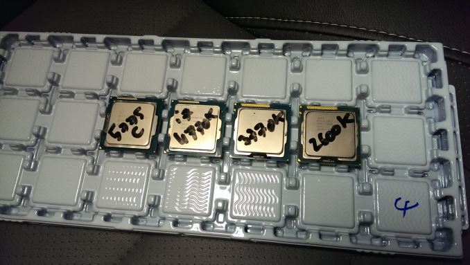
In our first part of our Broadwell coverage, we rushed to test both the i7-5775C and the i5-5765C in our new benchmarking suite against the previous generation of Haswell processors as well as AMDs Kaveri lineup. In Part 2, we have spent more time with the architecture to see how it stacks up against the last four years of Intel, as well as probing the high end overclocking capabilities.
Since our Part 1, the news mill from Intel has been an interesting mix of reduced revenue from the PC segments but a rise in expectation as we move from a dull Q2 into an exciting Q3 with back-to-school sales on the horizon and the release of Windows 10. Throw into the mix details about Intel's delayed 10nm process node, the injection of Kaby Lake processors after Skylake to break the tick tock model and it becomes an interesting next few years for the industry.
No matter the state of the tick-tock model (or what seems to be a tick-tock-tock with Kaby Lake), Intel's goals are still the same - improve efficiency of the main processor design and boost peak performance though instruction per clock (IPC) gains with each new processor design release. Simply stating you want an improvement in IPC and actually designing the semiconductor to get a boost in performance are two opposite ends of the difficulty spectrum.
Broadwell vs. Haswell
Intel's line of Haswell (4th generation) processors were released in June 2013, with a small updated design called Haswell Refresh in mid-2014 with improved frequencies and a small a package upgrade to benefit temperatures. Haswell is the name of the architecture, updating from the architecture on Ivy Bridge but on the same 22nm process node as Ivy Bridge. An architecture update incorporates a numerical of things - either a paradigm shift in the underlying semiconductor design, or a step up from the previous orientation by aiming for the low hanging fruit (times which can be updated for the most gain and the least effort). As a result, architecture jumps usually produce big (5-25%) jumps in performance. This is a tock, to use Intel's nomenclature.
| Intel's Tick-Tock Cadence | |||||
| Microarchitecture | Process Node | Tick or Tock | Release Year | ||
| Conroe/Merom | 65nm | Tock | 2006 | ||
| Penryn | 45nm | Tick | 2007 | ||
| Nehalem | 45nm | Tock | 2008 | ||
| Westmere | 32nm | Tick | 2010 | ||
| Sandy Bridge | 32nm | Tock | 2011 | ||
| Ivy Bridge | 22nm | Tick | 2012 | ||
| Haswell | 22nm | Tock | 2013 | ||
| Broadwell | 14nm | Tick | 2014 | ||
| Skylake | 14nm | Tock | 2015 | ||
| Kaby Lake (link)? | 14nm | Tock | 2016 ? | ||
The other half of the equation is a tick, or the movement from a larger process node to a smaller process node. This is by and large a scaled reduction in the mask used for the processor, but there are potential benefits based on the die area of the components of the processor and the connections within. Moving down to a smaller node typically does not change the base hardware underneath, but optimizations are made based on that die area reduction. With this in mind, we typically see smaller benefits in performance (5-10%), but better improvements in power consumption due to smaller transistors needing less voltage (although this is a balance between higher leakage currents). Overall, the typical goal of a process node change is typically efficiency, making it favored in mobile platforms.
Moving from Haswell to Broadwell on the desktop is a process node change, migrating from 22nm on Haswell to 14nm on Broadwell. As a result, the first processors released under the Broadwell nomenclature were mobile focused (Core M), and the desktop end of the stack us the last one to be updated. Though the desktop side is more subtle than that - Intel has released mid-powered versions of the processor with high end integrated graphics, an approach normally reserved for mobile devices or integrated devices such as all-in-ones. Perhaps it is then unsurprising that when desktop processors are launched under the -S or -DT naming scheme, Broadwell on the desktop is part of the -H line, normally reserved for mobile processors.
We've commented on Broadwell's minor architecture adjustments over Haswell before. They focus on reducing cache misses and keeping more predicted operations in flight at any one time, reducing the need to move back out of memory and increase throughput. This is mostly achieved by exploiting the available area when function units are reduced in size from the node change - increasing the out-of-order scheduler size, increasing the L2 TLB to allow for both more local misses/larger memory jump requests, and the page miss handler doubles in size.

This, according to Intel, accounts for a 5% increase in IPC (instructions per clock) by focusing on reducing the wait time for data for the traditional CPU part of the Broadwell processor.
In our initial review of the Broadwell processors, we saw that it was not as straightforward as this. The two CPUs we tested, the i7-5775C and the i5-5675C, are built to a 65W thermal design power, compared to the high end models from Haswell which are at the 84/88W level. This means that for users looking for the next most powerful processor, the base processor frequencies of the Broadwell samples we had are lower and less performant due to frequency, more than any IPC increase could overcome.
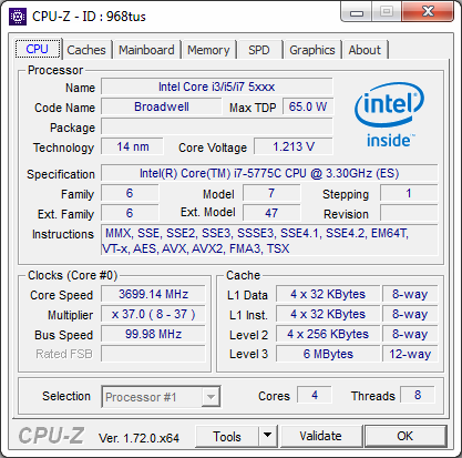
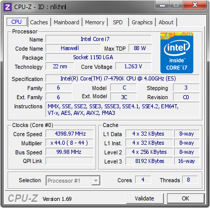
Core i7-5775C lining up with the Core i7-4790K
It was difficult for Broadwell to win any CPU focused benchmark from a pure frequency (and TDP) handicap. To add an additional element into the mix, almost every Broadwell's memory cache system is also different:
| Intel Desktop Processor Cache Comparison | |||||
| L1-D | L1-I | L2 | L3 | L4 | |
| Sandy Bridge i7 | 4 x 32 KB | 4 x 32 KB | 4 x 256 KB | 8 MB | |
| Ivy Bridge i7 | 4 x 32 KB | 4 x 32 KB | 4 x 256 KB | 8 MB | |
| Haswell i7 | 4 x 32 KB | 4 x 32 KB | 4 x 256 KB | 8 MB | |
| Broadwell i7 (Desktop / Iris Pro 6200) |
4 x 32 KB | 4 x 32 KB | 4 x 256 KB | 6 MB | 128 MB eDRAM |
|
|
|||||
| Haswell i5 | 4 x 32 KB | 4 x 32 KB | 4 x 256 KB | 6 MB | |
| Broadwell i7 (i7-5700HQ / HD 5600) |
4 x 32 KB | 4 x 32 KB | 4 x 256 KB | 6 MB | |
Both the Level 1 and Level 2 caches of each processor are the same, but at Level 3 where Haswell i7 has 8MB, the Broadwell i7 only has 6MB. Aside from the improved branch predictor mentioned above to reduce cache misses, Broadwell also has a separate eDRAM in the CPU package, weighing in at 128MB. This acts as a level 4 cache, having a latency between the L3 and moving out to memory, resulting in less trips out to main memory. This combination of architecture improvements and eDRAM on Broadwell combined with the lower L3 cache size makes it an unknown in memory performance.
I have also included the Haswell i5 and the Broadwell-based i7-5700HQ in this table, showing that the Broadwell i7 L1/L2/L3 cache hierarchy is more akin to a desktop i5 processor and that Broadwell is available without the eDRAM. That being said, the i7-5700HQ is a single processor destined for laptops, making any discrete testing nominally impossible, and taken out of the real-world context for the majority of Broadwell desktop owners.
The reason for Broadwell's eDRAM comes from Intel's ‘Crystal Well’ strategy. Crystal Well is a designation given to a processor which has this eDRAM (and typically a larger integrated graphics package as well). Integrated graphics are historically inhibited by memory bandwidth, having to almost always reach out to main memory to process textures in graphic workloads. The eDRAM allows more data to be stored between the graphics core and the memory, and at a higher memory bandwidth, potentially improving output. By combining the high end integrated graphics with the eDRAM, Intel created these Broadwell processors as the fastest integrated graphics solution available on a socketable (replaceable processor) platform.
That being said, due to Broadwell being the latest product from Intel, and it having the most recent (and expensive) process node, equipped with eDRAM which is a separate die on the package, the Broadwell solutions do not come cheap. The pricing is almost in line with previous Haswell mainstream i7 processors, albeit at the lower thermal design and the beefier integrated graphics. As we determined in the Broadwell Part 1 review, the desktop Broadwell has the absolute integrated performance crown, although an AMD APU system will be significantly more cost effective. Both platforms are hoping that multi-GPU possibilities in DirectX12 have a positive outcome to their solutions.
This Review
We said we'd be back for part 2, and this is it. Here I wanted to cover what we couldn't previously due to early BIOS revisions and limited time testing - specifically looking at how Broadwell performs when overclocking, and whether the Broadwell architecture is truly a step up over previous generations of Intel processors. In the last review our comparison point was the i7-4770K from Intel's Haswell line; for part two we also back tested the i7-3770K from the Ivy Bridge platform and the i7-2600K from Sandy Bridge, covering the four most recent Intel processor architectures dating back to January 2011. We also have data on older benchmarks going back further. All four of the most recent architectures are tested at their stock speeds and at a constant 3 GHz (at 1866 C9) to find how IPC improves. (Incidentally I did find an i7-750 and a Q9550 in my CPU bin for the next two generations back, but have no motherboards for testing our more recent benchmarks. I'll see what I can put together for a mini-piece later in the year.)
Test setup
| Test Setup | |||||||||||||||||||||
| Processor |
|
||||||||||||||||||||
| Motherboards | MSI Z97A Gaming 6 (LGA1150) ASRock Z77 OC Formula (LGA1155) |
||||||||||||||||||||
| Cooling | Cooler Master Nepton 140XL | ||||||||||||||||||||
| Power Supply | OCZ 1250W Gold ZX Series | ||||||||||||||||||||
| Memory | G.Skill RipjawsZ 4x4 GB DDR3-1866 9-11-11 Kit | ||||||||||||||||||||
| Video Cards | ASUS GTX 980 Strix 4GB MSI GTX 770 Lightning 2GB (1150/1202 Boost) ASUS R7 240 2GB |
||||||||||||||||||||
| Hard Drive | Crucial MX200 1TB | ||||||||||||||||||||
| Optical Drive | LG GH22NS50 | ||||||||||||||||||||
| Case | Open Test Bed | ||||||||||||||||||||
| Operating System | Windows 7 64-bit SP1 | ||||||||||||||||||||
Many thanks to
Thank you to AMD for providing us with the R9 290X 4GB GPUs.
Thank you to ASUS for providing us with GTX 980 Strix GPUs and the R7 240 DDR3 GPU.
Thank you to ASRock and ASUS for providing us with some IO testing kit.
Thank you to Cooler Master for providing us with Nepton 140XL CLCs.
Thank you to Corsair for providing us with an AX1200i PSU.
Thank you to Crucial for providing us with MX200 SSDs.
Thank you to G.Skill and Corsair for providing us with memory.
Thank you to MSI for providing us with the GTX 770 Lightning GPUs.
Thank you to OCZ for providing us with PSUs.
Thank you to Rosewill for providing us with PSUs and RK-9100 keyboards.


121 Comments
View All Comments
TheinsanegamerN - Monday, August 3, 2015 - link
Quite nice comparison.Unfortunately, it seems that, while broadwell does have the best IPC of the bunch, the overclock is pathetic. 1.325v to hit 4.2 GHz? my ivy bridge 3570k does the same clock with 1.075v. now, I've been told I have a exceptionally good chip, but it strikes me as odd that broadwell, being on a smaller 14nm process, cant match what ivy bridge could do two years ago. and since sandy bridge can be OC'ed to 4.7GHz+ with ease,and ive can hit 4.5, it seems there is still no reason to upgrade to broadwell, as any IPC gains are cancelled out by the lower clock rate. unless you need to do lots of dolphin emulation and refuse to overclock at all, the ancient sandy bridge still seems to do the best.
K_Space - Monday, August 3, 2015 - link
TheinsanegamerN agreed. Those who held into their Sandy made a very wise investment, just like those good ol' 920s back in the X58 era.Dupl3xxx - Monday, August 3, 2015 - link
Ah, yes, the 920 was a lovely beast. Started overclocking at 3.6. It booted, tried 3.8, booted, tried 4.0, failed. 3.8 was literally done in less than an hour as my second ever attempt at overclocking, with my first being the intel e6600. And when a dying PSU wounded it, I got a 3930k. It does 4.0 ghz, and I've yet to find any situation where it's a bottleneck, besides things like rendering and benchmarks. I considered upgrading to the 59xx series, but when I learned that only the 5960x would be a 8-core, that was quickly decided against.It'll be interesting to watch Skylake and Zen fight it out in a year or so.
Impulses - Monday, August 3, 2015 - link
I'm surprised Intel isn't banking on nostalgic memories of the Q6600 to hype the 6600K & 6700K... Surely marketing had a hand in the simplified naming reminiscent of the old C2Q.augiem - Monday, August 3, 2015 - link
I'm still on a i7-920 from mid 2009. Been running 3.6GHz the entire time, still rock solid as the day I bought it. I still can't believe I've been using a PC for this long. Before the i7, I would upgrade every 1.5 - 2 years tops. This thing is nuts.mkozakewich - Tuesday, August 4, 2015 - link
We've reached the end of that exponential advancement, so you can expect things to advance at roughly this rate for a while, at least until we also reach "small enough".close - Tuesday, August 4, 2015 - link
That's logarithmic advancement :). It keeps slowing down year after year.Cryio - Tuesday, August 4, 2015 - link
Technically with Sandy Bridge they reached the end. SB was quite a jump over Nehalem.Harry Lloyd - Tuesday, August 4, 2015 - link
There is no end. Intel just do not care, as they have no competition. Why would they waste money on increasing performance, when they can focus on efficiency for mobile? They can get away with selling basically the same CPUs every year on desktop, as they are still the fastest.Badelhas - Tuesday, August 4, 2015 - link
I also blame AMD. If they had good high end CPUs Intel would be forced to improve the ones they´ve been selling for the last 5 years or so.