SK hynix Announces 238 Layer NAND - Mass Production To Start In H1'2023
by Ryan Smith on August 4, 2022 8:00 AM EST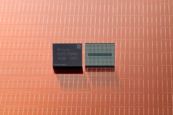
As the 2022 Flash Memory Summit continues, SK hynix is the latest vendor to announce their next generation of NAND flash memory at the show. Showcasing for the first time the company’s forthcoming 238 layer TLC NAND, which promises both improved density/capacity and improved bandwidth. At 238 layers, SK hynix has, at least for the moment, secured bragging rights for the greatest number of layers in a TLC NAND die – though with mass production not set to begin until 2023, it’s going to be a while until the company’s newest NAND shows up in retail products.
Following closely on the heels of Micron’s 232L TLC NAND announcement last week, SK hynix is upping the ante ever so slightly with a 238 layer design. Though the difference in layer counts is largely inconsequential when you’re talking about NAND dies with 200+ layers to begin with, in the highly competitive flash memory industry it gives SK hynix bragging rights on layer counts, breaking the previous stalemate between them, Samsung, and Micron at 176L.
From a technical perspective, SK hynix’s 238L NAND further builds upon the basic design of their 176L NAND. So we’re once again looking at a string stacked design, with SH hynix using a pair of 119 layer decks, up from 88 layers in the previous generation. This makes SK hynix the third flash memory vendor to master building decks over 100 layers tall, and is what’s enabling them to produce a 238L NAND design that holds the line at two decks.
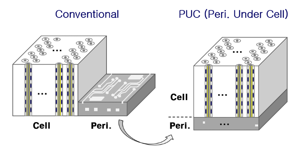
SK hynix’s NAND decks continue to be built with their charge-trap, CMOS under Array (CuA) architecture, which sees the bulk of the NAND’s logic placed under the NAND memory cells. According to the company, their initial 512Gbit TLC part has a die size of 35.58mm2, which works out to a density of roughly 14.39 Gbit/mm2. That’s a 35% improvement in density over their previous-generation 176L TLC NAND die at equivalent capacities. Notably, this does mean that SK hynix will be ever so slightly trailing Micron’s 232L NAND despite their total layer count advantage, as Micron claims they’ve hit a density of 14.6 Gbit/mm2 on their 1Tbit dies.
| SK hynix 3D TLC NAND Flash Memory | ||
| 238L | 176L | |
| Layers | 238 | 176 |
| Decks | 2 (x119) | 2 (x88) |
| Die Capacity | 512 Gbit | 512 Gbit |
| Die Size (mm2) | 35.58mm2 | ~47.4mm2 |
| Density (Gbit/mm2) | ~14.39 | 10.8 |
| I/O Speed | 2.4 MT/s (ONFi 5.0) |
1.6 MT/s (ONFI 4.2) |
| CuA / PuC | Yes | Yes |
Speaking of 1Tbit, unlike Micron, SK hynix is not using the density improvements to build higher capacity dies – at least, not yet. While the company has announced that they will be building 1Tbit dies next year using their 238L process, for now they’re holding at 512Gbit, the same capacity as their previous generation. So all other factors held equal, we shouldn’t expect the first wave drives built using 238L NAND to have any greater capacity than the current generation. But, if nothing else, at least SK hynix’s initial 238L dies are quite small – though whether that translates at all to smaller packages remains to be seen.
Besides density improvements, SK hynix has also improved the performance and power consumption of their NAND. Like the other NAND vendors, SK hynix is using this upcoming generation of NAND to introduce ONFi 5.0 support. ONFi 5.0 is notable for not only increasing the top transfer rate to 2400MT/second – a 50% improvement over ONFi 4.2 – but it also introduces a new NV-LPDDR4 signaling method. As it’s based on LPDDR signaling (unlike the DDR3-derrived mode in ONFi 4.x), NV-LPDDR4 offers tangible reductions in the amount of power consumed by NAND signaling. SK hynix isn’t breaking their power consumption figures out to this level of detail, but for overall power consumption, they’re touting a 21% reduction in energy consumed for read operations. Presumably this is per bit, so it will be counterbalanced by the 50% improvement in bandwidth.
This week’s announcement comes as SK hynix has begun shipping samples of the 238L NAND to their customers. As previously mentioned, the company is not planning on kicking off mass production until H1’2023, so it will be some time before we see the new NAND show up in retail products. According to SK hynix, their plan is to start with shipping NAND for consumer SSDs, followed by smartphones and high-capacity server SSDs. That, in turn, will be followed up with the introduction of 1Tbit 238L NAND later in 2023.
Source: SK hynix


7 Comments
View All Comments
Ashinjuka - Thursday, August 4, 2022 - link
can't wait for quintLC and hexLCLiKenun - Saturday, August 6, 2022 - link
Mixing Latin and Greek, I see. 🙂“pent-” (5, Greek)
“quin-” (5, Latin)
“hex-” (6, Greek)
“sex-” (6, Latin)
Stick with Greek and you get viable three-letter abbreviations up to 6.
“hept-” (7, Greek)
“sept-” (7, Latin)
You can see how it stops working for either prefix at 7.
ballsystemlord - Thursday, August 4, 2022 - link
Are the ONFi standards open, or closed?Unashamed_unoriginal_username_x86 - Monday, August 8, 2022 - link
looks like they are, pleasantly surprised by how surprisingly pleasant their page is. Good summaries of the standards:http://www.onfi.org/specifications/
Unashamed_unoriginal_username_x86 - Monday, August 8, 2022 - link
Also apparently it stands for Open NAND Flash interface, so there you have itFunBunny2 - Saturday, August 6, 2022 - link
It was an article of faith when 3D flash began that TLC (and Q and whatever comes next) would be built on much larger (ancestor) nodes, thus keeping, or even increasing, durability as bit density went up.but, in due time, the cynics amongst us disabused us of this idea. the vendors would push these multi-value cells into current node sizes, and thus reduce erase cycles into double digits. any information on that aspect?
artifex - Sunday, August 7, 2022 - link
I wonder how they handle heat dissipation compared to their 176L modules.