Intel 3rd Gen Xeon Scalable (Ice Lake SP) Review: Generationally Big, Competitively Small
by Andrei Frumusanu on April 6, 2021 11:00 AM EST- Posted in
- Servers
- CPUs
- Intel
- Xeon
- Enterprise
- Xeon Scalable
- Ice Lake-SP
Section by Ian Cutress
The launch of Intel’s Ice Lake Xeon Scalable processors has been in the wings for a number of years. The delays to Intel’s 10nm manufacturing process have given a number of setbacks to all of Intel’s proposed 10nm product lines, especially the high performance Xeon family: trying to craft 660 mm2 of silicon on a process is difficult at the best of times. But Intel has 10nm in a place where it is economically viable to start retailing large Xeon processors, and the official launch today of Intel’s 3rd Generation Xeon Scalable is on the back of over 200,000+ units shipped to major customers to date. The new flagship, the Xeon Platinum 8380, has 40 cores, offers PCIe 4.0, and takes advantage of the IPC gain in Intel’s Sunny Cove processor core. We’re testing it against the best in the market.
Intel’s 3rd Generation Xeon Scalable: 10nm Goes Enterprise
Today Intel is launching the full stack of processors under the 3rd Generation Xeon Scalable Ice Lake branding, built upon its 10nm process. These processors, up to 40 cores per socket, are designed solely for single socket and dual socket systems, competing in a market with other x86 and Arm options available. With this new generation, Intel’s offering is aimed to be two-fold: first, the generational uplift compared to 2nd Gen, but also the narrative around selling a solution rather than simply selling a processor.
Intel’s messaging with its new Ice Lake Xeon Scalable (ICX or ICL-SP) steers away from simple single core or multicore performance, and instead is that the unique feature set, such as AVX-512, DLBoost, cryptography acceleration, and security, along with appropriate software optimizations or paired with specialist Intel family products, such as Optane DC Persistent Memory, Agilex FPGAs/SmartNICs, or 800-series Ethernet, offer better performance and better metrics for those actually buying the systems. This angle, Intel believes, puts it in a better position than its competitors that only offer a limited subset of these features, or lack the infrastructure to unite these products under a single easy-to-use brand.
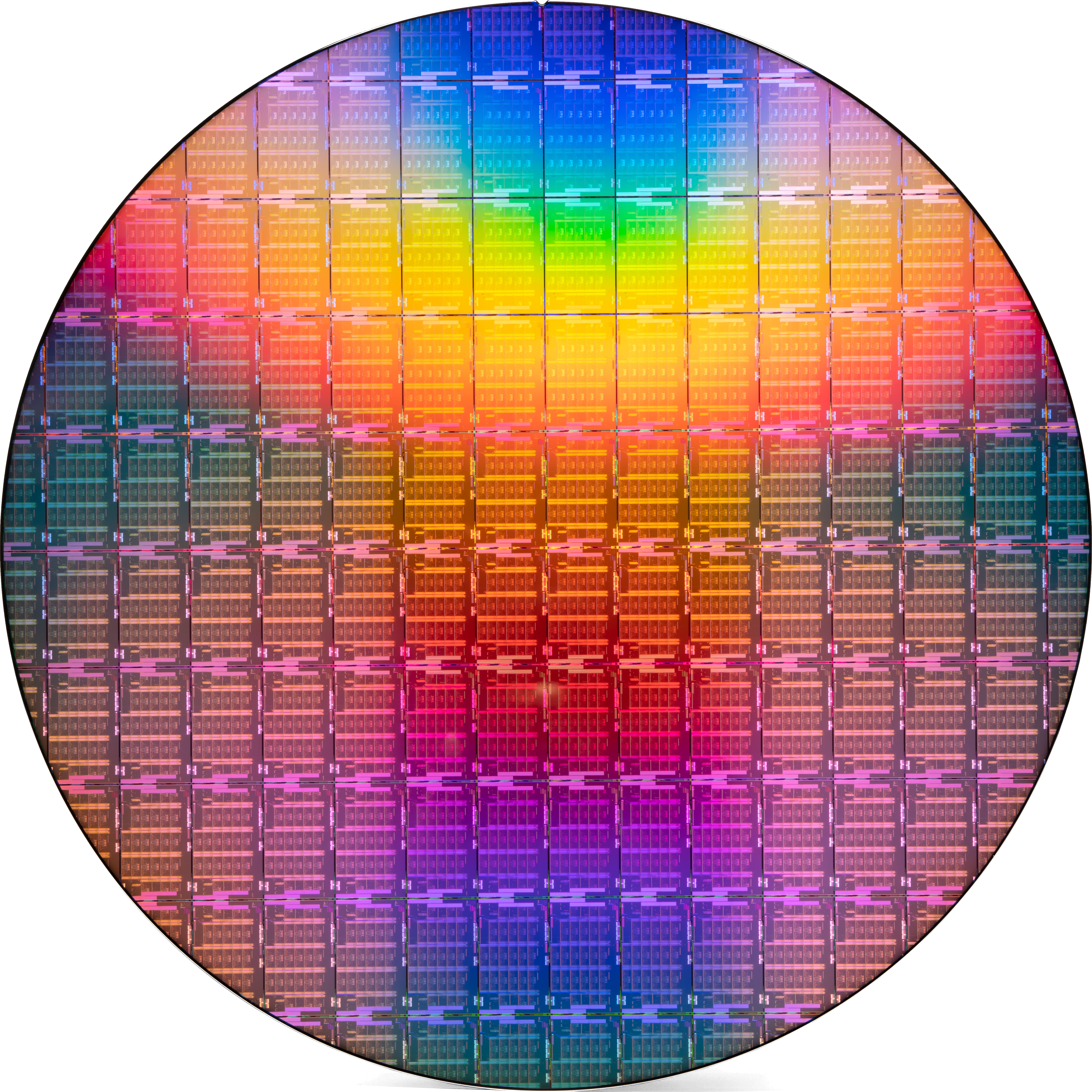
An Wafer of 40-core Ice Lake Xeon 10nm Processors
Nonetheless, the launch of a new generation of products and an expanded portfolio warrants the product to actually be put under test for its raw base performance claims. This generation of Xeon Scalable, Intel’s first on 10nm, uses a newer architecture Sunny Cove core. Benefits of this core, as explained by Intel, start with an extra 20% raw performance increase, enabled through a much wider core with an improved front end and a more execution resources. Outside of the core, memory bandwidth is improved both by increasing memory channels from six to eight, but also new memory prefetch techniques and optimizations that increases bandwidth up to 100% with another +25% efficiency. The mesh interconnect between the cores also uses updated algorithms to feed IO to and from the cores, and Intel is promoting better power management through independent power management agents inside each IP block.
On top of this, Intel is layering on accelerative features, stating that over the raw performance, software optimized for these accelerators will see a better-than-generational uplift. This starts with the basic core layout, especially as it pertains to SIMD commands such as SSSE, AVX, AVX2, and AVX-512: Intel is enabling better cryptography support across its ISA, enabling AES, SHA, GFNI, and other instructions to run simultaneously across all vector instruction sets. AVX-512 has improved frequencies during more complex bit operations for ICX with smarter mapping between instructions and power draw, offering an extra 10% frequency for all 256-bit instructions. On top of this is Intel’s Speed Select Technologies, such as Performance Profile, Base Frequency improvements, Turbo Frequency improvements, and Core Power assistance to ensure peak per-core performance or quality of service during a heavily utilized system depending on customer requirements. Other new features include Software Guard Extensions, enabling enclave sizes up to 512 GB per socket with select models.
Ice Lake’s Sunny Cove Core: Part 2
The Sunny Cove core has actually already been in the market. Intel has made a consumer variant of the core and a server variant of the core. Ice Lake Xeon has the server variant, with bigger caches and slightly different optimization points, but it’s the consumer variant that we have seen and tested in laptop form. Sunny Cove is part of Intel’s Ice Lake notebook processor portfolio, which we reviewed the performance back on August 1st 2019, which 614 days ago. That length of time between enabling a core for notebooks and enabling the same core (with upgrades for servers) on enterprise is almost unheard of, but indicative of Intel’s troubles in manufacturing.
Nonetheless, in our notebook testing of the Ice Lake core, we saw a raw +17-18% performance over the previous generation, however this was at the expense of 15-20% in frequency. Where the product truly excelled was in memory limited scenarios, where a new memory controller provided better-than-generational uplift. When it comes to this generation of Xeon Scalable processors with the new core, as you see in the review, in non-accelerated workloads we get very much a similar story. That being said, consumer hardware is very often TDP limited, especially laptops! With the new Ice Lake Xeon platform, Intel is boosting the peak TDP from 205 W to 270 W, which also gives additional performance advantages.
The Headline Act: Intel’s Xeon Platinum 8380
The head prefect of Intel’s new processor lineup is the Platinum 8380 - a full fat 40 core behemoth. If we put it side by side with the previous generation processors, there some key specifications to note.
| Intel Xeon Comparison: 3rd Gen vs 2nd Gen Peak vs Peak |
||
| Xeon Platinum 8380 |
AnandTech | Xeon Platinum 8280 |
| 40 / 80 | Cores / Threads | 28 / 56 |
| 2900 / 3400 / 3000 | Base / ST / MT Freq | 2700 / 4000 / 3300 |
| 50 MB + 60 MB | L2 + L3 Cache | 28 MB + 38.5 MB |
| 270 W | TDP | 205 W |
| PCIe 4.0 x64 | PCIe | PCIe 3.0 x48 |
| 8 x DDR4-3200 | DRAM Support | 6 x DDR4-2933 |
| 4 TB | DRAM Capacity | 1 TB |
| 200-series | Optane | 100-series |
| 4 TB Optane + 2 TB DRAM |
Optane Capacity Per Socket |
1 TB DDR4-2666 + 1.5 TB |
| 512 GB | SGX Enclave | None |
| 1P, 2P | Socket Support | 1P, 2P, 4P, 8P |
| 3 x 11.2 GT/s | UPI Links | 3 x 10.4 GT/s |
| $8099 | Price (1ku) | $10099* 6258R, 2P Variant is only $3950 |
Between these processors, the new flagship has a number of positives:
- +43% more cores (40 vs 28),
- nearly double the cache,
- +33% more PCIe lanes (64 vs 48),
- 2x the PCIe bandwidth (PCIe 4.0 vs PCIe 3.0)
- 4x the memory support (4 TB vs 1 TB)
- SGX Enclave support
- +7% higher socket-to-socket bandwidth
- Support for DDR4-3200 Optane DCPMM 200-series
- Price is down 20%... or up 100% if you compare to 6258R
Though we should perhaps highlight some of the negatives:
- TDP is up +32% (270 W vs 205 W)
- ST Frequency is down (3400 MHz vs 4000 MHz)
- MT Frequency is down (3000 MHz vs 3300 MHz)
If we combine the specification sheet cores and all-core (MT) frequency, Ice Lake actually has about the same efficiency here as the previous generation. Modern high-performance processors often operate well outside the peak efficiency window, however Ice Lake being at a lower frequency would usually suggest that Ice Lake is having to operate closer to the peak efficiency point to stay within a suitable socket TDP than previous generations. This is similar to what we saw in the laptop space.
Features across all Ice Lake Xeon Scalable processors
We’ll dive into the different processors over on the next page, however it is worth noting some of the key features that will apply to all of Intel’s new ICL-SP family. Across the ~40 new processors, including all the media focused parts, the network focused processors, and all the individual optimizations used, all of the processors will have the following:
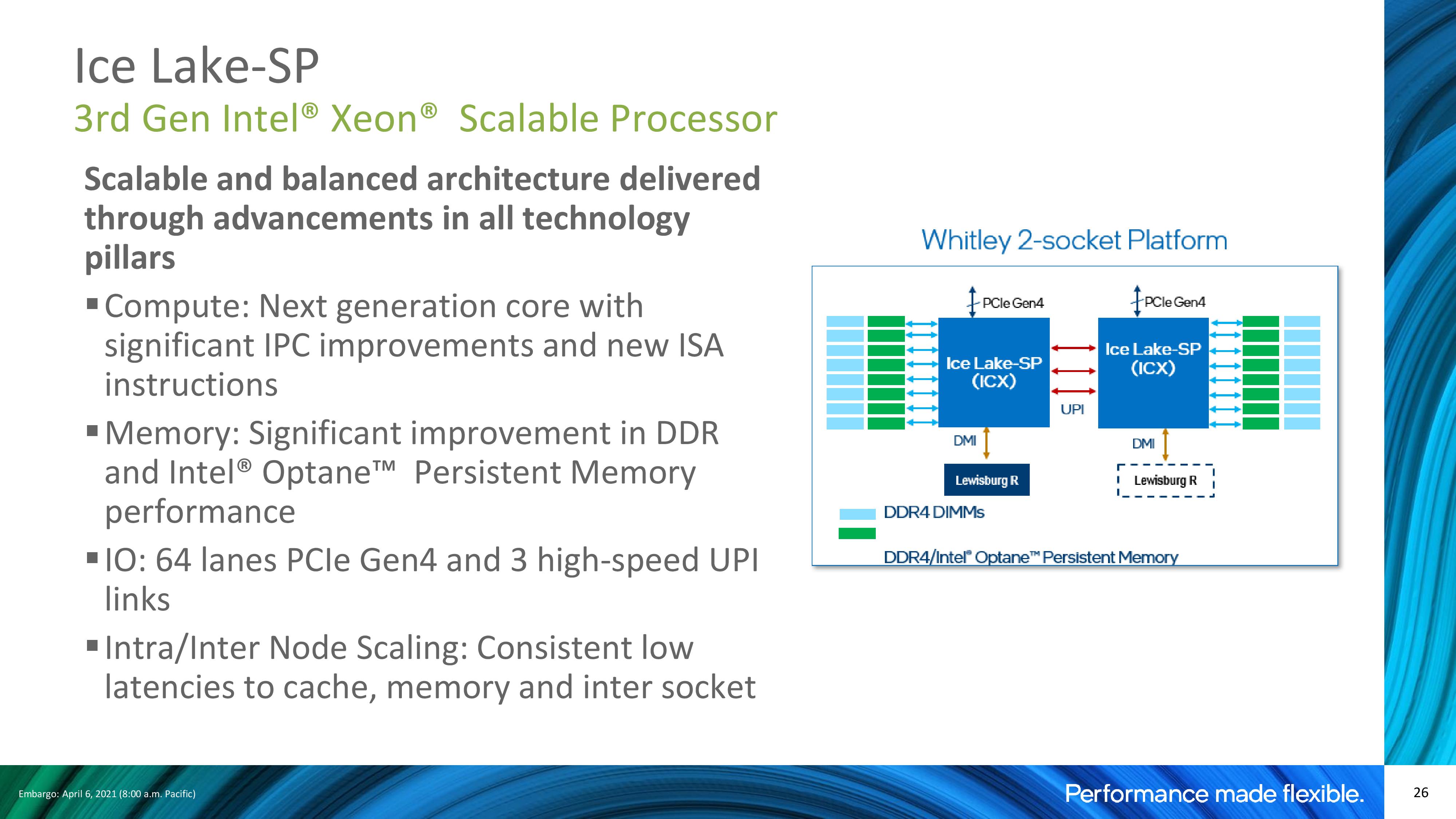
All Ice Lake Xeons will support eight channels of DDR4-3200 at 2DPC(new info)- All Ice Lake Xeons will support 4 TB of DRAM per socket
- All Ice Lake Xeons will support SGX Enclaves (size will vary)
- All Ice Lake Xeons will support 64x PCIe 4.0 lanes
- All Ice Lake Xeons will support 2x FMA
- Platinum/Gold Xeons will support 3x UPI links at 11.2 GT/s, Silver is 2x links at 10.4 GT/s
- Platinum/Gold Xeons will support 200-series Optane DC Persistent Memory
In the past, Intel has often productized some of these features at will sell the ones that are more capable at a higher cost. This segmentation is often borne from a lack of competition in the market. This time around however, Intel has seen fit to unify some of its segmentation for consistency. The key one in my mind is memory support: at the start of the Xeon Scalable family, Intel started to charge extra for high-capacity memory models. But in light of the competition now offering 4 TB/socket at no extra cost, it would appear that Intel has decided to unify the stack with one memory support option.
Intel 3rd Generation Xeon Scalable: New Socket, New Motherboards
Ice Lake Xeons, now with eight memory channels rather than six, will require a new socket and new motherboards. Ice Lake comes with 4189 pins, and requires an LGA4189-4 ‘Whitley’ motherboard. This is different to the LGA4189-5 ‘Cedar Island’ in use for Cooper Lake, and the two are not interoperable, however they do share a power profile.
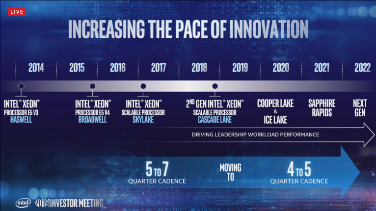
This actually brings us onto a point about Intel’s portfolio. Technically 10nm Ice Lake is not the only member of the 3rd Gen Xeon Scalable family – Intel has seen fit to bundle both 14nm Cooper Lake and 10nm Ice Lake under the same heading. Intel is separating the two by stating that Cooper Lake is focused at several specific high volume customers looking to deploy quad-socket and eight-socket systems with specific AI workloads. By comparison, Ice Lake is for the mass market, and limited to two socket systems.
Ice Lake and Cooper Lake both have the ‘3’ in the processor name indicating third generation. Users can tell which ones are Cooper Lake because they end in either H or HL – Ice Lake processors (as we’ll see on the next page) never have H or HL. Most Cooper Lake processors are Platinum models anyway, with a few Xeon Gold. As we go through this review, we’ll focus solely on Ice Lake, given that this is the platform Intel is selling to the mainstream.
This Review
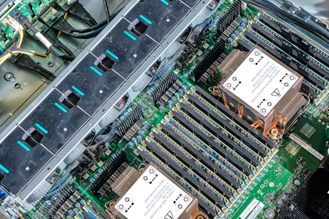
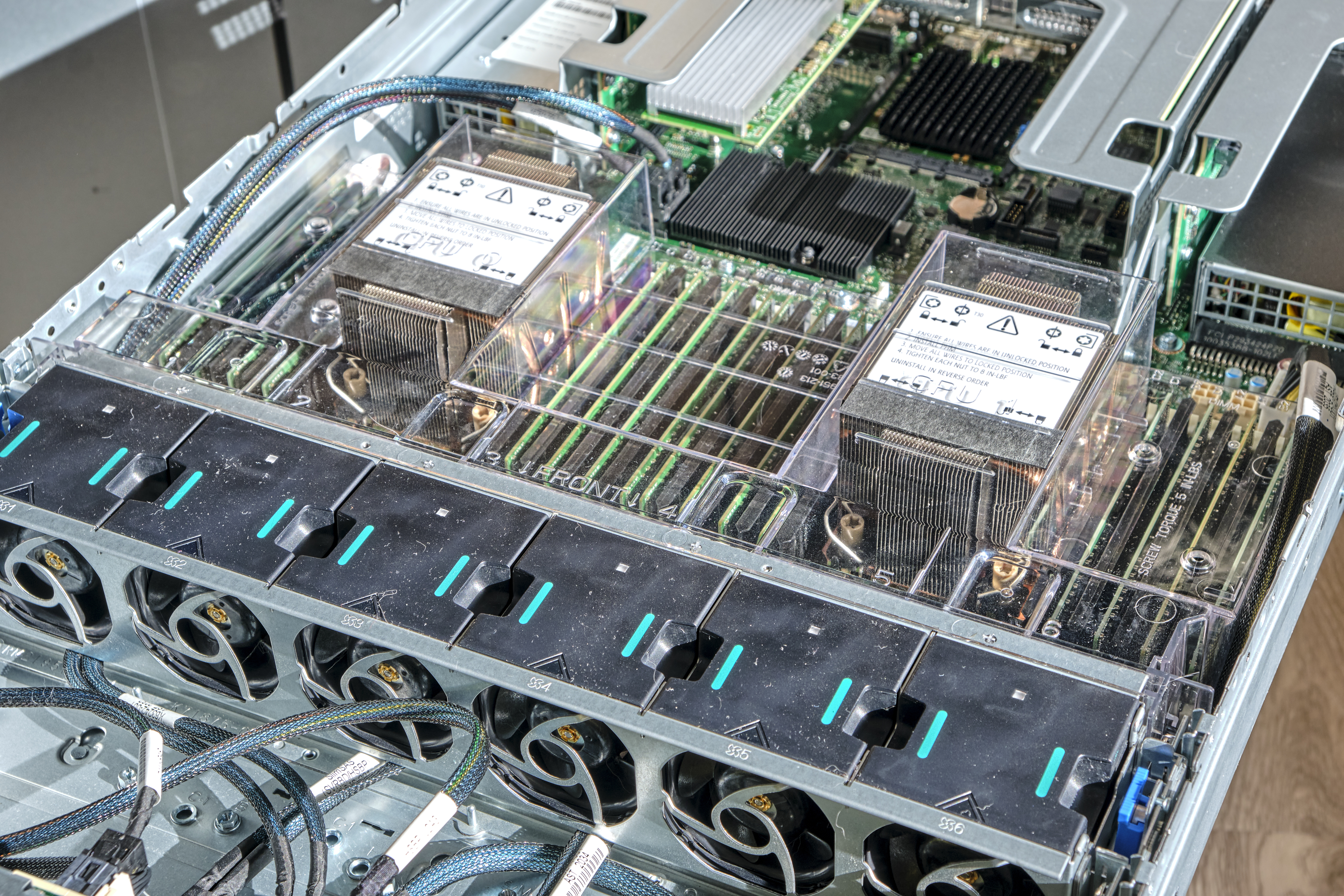
In the lead up to this launch today, Intel provided us with a 2U system featuring two of the top models of Ice Lake Xeon: we have dual 40 core Xeon Platinum 8380s! At the same time, we have also spent time a dual Xeon Gold 6330 system from Supermicro, which has two 28-core processors, and acts as a good comparison to the previous generation Xeon Platinum 8280.
Our review today will cover the processor stack, our benchmarks, power analysis, memory analysis, and some initial conclusions.


169 Comments
View All Comments
deil - Tuesday, April 6, 2021 - link
that's a lot of upgrade for intelGomez Addams - Tuesday, April 6, 2021 - link
That is a curious-looking wafer. I thought it was fake at first but then I noticed the alignment notch. Actually, I'm still not convinced it's real because I have seen lots and lots of wafers in various stages of production and I have never seen one where partial chips go all the way out to the edges. It's a waste of time to deal with those in the steppers so no one does that.JCB994 - Tuesday, April 6, 2021 - link
Periphery defects? I used to deal with those...buildup of material that would breakdown during wet processing and stream particles all over the wafer. Running partials as far out as possible helped. Nowadays...do they still use big wet benches? I have been out awhile...Gomez Addams - Tuesday, April 6, 2021 - link
Yes, they do. That's one of the systems I spent lots of time working on. Those don't look defects to me. They are just a continuation of the chip pattern.FullmetalTitan - Saturday, April 24, 2021 - link
Still the most chemical efficient tools for some etch processes. It is odd to see die prints out to the edge all around, usually at least the 'corners' are inked out/not patterned by the time it hits copper layers because printing features out that far can increase the chances of film delamination, which just leads to more defectivity. I suppose on DUV tools the extra few seconds to run those shots isn't THAT bad on non-immersion layers, but it adds up over timeArsenica - Tuesday, April 6, 2021 - link
It isn´t real if it doesn´t have DrIan bite marks./jk
ilt24 - Tuesday, April 6, 2021 - link
@Gomez AddamsI spent my entire career working in the semiconductor industry, although in IT, and I have seen many wafers from 4" to 12" and printing partial die off the edge of the wafer is quite common.
check out the pictures in these article:
https://www.anandtech.com/show/15380/i-ran-off-wit...
https://www.anandtech.com/show/9723/amd-to-spinoff...
Kamen Rider Blade - Tuesday, April 6, 2021 - link
So when are we going to hit 450 mm / 18" waffers?Are we ever going to get Hexagonal Die's to maximize possible Yields?
http://www.semiconductor-today.com/news_items/2020...
https://semiaccurate.com/2015/05/18/disco-makes-he...
They can already do that for simple LED's, but trying to bring Hexagonal IC Dies into existence is going to be exciting because there is a theoretical 62.5% increase in Manufactured Dies for a given Waffer Diameter and using Hexagonal IC Dies of a similar/identical area.
ilt24 - Tuesday, April 6, 2021 - link
@Kamen Rider Blade - "So when are we going to hit 450 mm / 18" waffers?"It seems the desire to move to EUV distracted TSMC, Samsung and Intel who are probably the only companies that were really interested in 450mm.
saratoga4 - Tuesday, April 6, 2021 - link
>So when are we going to hit 450 mm / 18" waffers?For logic, never since there is little to no advantage to larger wafers. Possibly NAND might use it, but we'll see if its even worth it there.
>Are we ever going to get Hexagonal Die's to maximize possible Yields?
Probably not for logic. With reticle sizes getting smaller in the coming nodes, it makes even less sense going forward then it did in the past, and it didn't make much sense then to begin with.