IBM at FMS 2020: Beating TLC With QLC, MRAM And Computational Storage
by Billy Tallis on November 12, 2020 8:00 AM EST- Posted in
- SSDs
- Storage
- Enterprise SSDs
- IBM
- NVMe
- Flash Memory Summit
- QLC NAND
- Everspin
- MRAM
Two years ago we reported on IBM's FlashCore Module, their custom U.2 NVMe SSD for use in their FlashSystem enterprise storage appliances. Earlier this year IBM released the FlashCore Module 2 and this week they detailed it in a keynote presentation at Flash Memory Summit. Like its predecessor, the FCM 2 is a very high-end enterprise SSD with some unusual and surprising design choices.
The most unusual feature of the first IBM FlashCore Module was the fact that it did not use any supercapacitors for power loss protection, nor did the host system include battery backup. Instead, IBM included Everspin's magnetoresistive RAM (MRAM) to provide an inherently non-volatile write cache. The FCM 2 continues to use MRAM, now upgraded from Everspin's 256Mbit ST-DDR3 to their 1Gbit ST-DDR4 memory. The higher-density MRAM makes it much easier to include a useful quantity on the drive, but it's still far too expensive to entirely replace DRAM on the SSD: managing the FCM2's multi-TB capacities require several GB of RAM. IBM's main motivation for using MRAM as a write buffer instead of DRAM with power loss protection is that supercaps or batteries tend to have service lifespans of only a few years, and when an energy storage system fails things can get ugly. IBM sees MRAM as offering better long-term reliability that is worth the cost and complexity of building a drive with three kinds of memory.

The FCM 1 used Micron 64-layer 3D TLC NAND, which at the time was a pretty standard choice for high-end enterprise SSDs. The FCM 2 makes the bold switch to using Micron's 96L 3D QLC NAND. The higher density and lower cost per bit has enabled them to double the maximum drive capacity up to 38.4 TB, but maintaining performance while using inherently slower flash is a tall order. Fundamentally, the new NAND has about three times the program (write) latency and 2-3 times the read latency. Write endurance and data retention are also lower. But the FCM 2 is still rated for 2 DWPD and IBM claims increased performance thanks to a combination of several tricks.
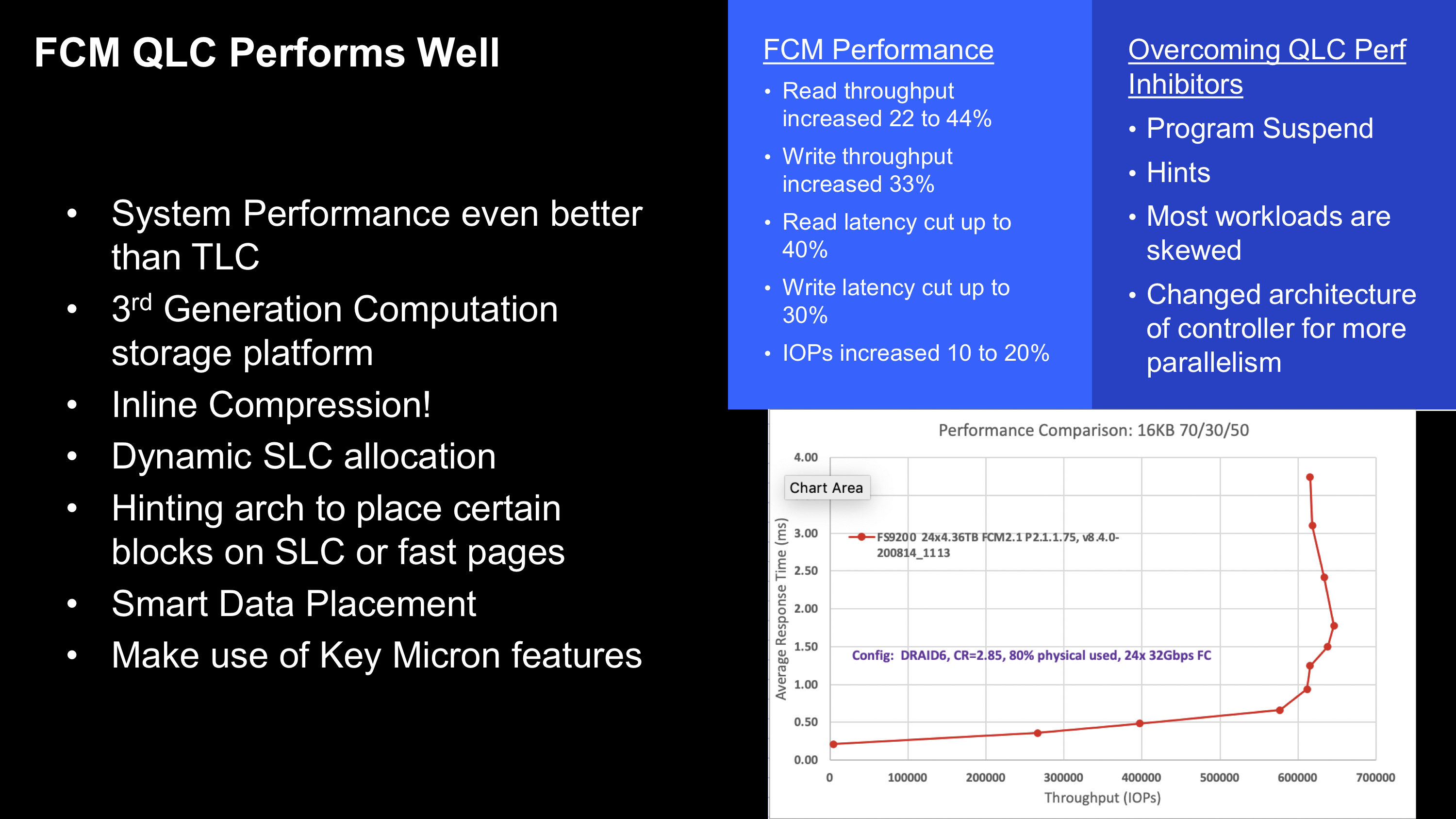
IBM's FlashCore Modules use a custom SSD controller architecture implemented on a massive FPGA. The 20-channel NAND interface explains the slightly odd drive capacities compared to more run of the mill SSDs with 8 or 16 channel controllers. IBM includes line-rate transparent compression derived from the hardware compression provided on IBM Z mainframes. This provides a compression ratio around 2.3x on typical data sets, which goes a long way toward mitigating the endurance issues with QLC (but the FCM 1 also had compression, so this isn't a big advantage for the FCM 2). The FCM 2 also can use some of its QLC NAND as SLC. This isn't as simple as the SLC write caches found on virtually all consumer SSDs. Instead, the FCM 2 tracks IO patterns to predict which chunks of data will be frequently accessed ("hot" data), and tries to store those on SLC instead of QLC while sending "cold" data straight to QLC. Enterprise SSDs typically avoid using SLC caching because it makes it hard to ensure good QoS during sustained workloads. (Client drives can count on real-world workloads offering plenty of idle time that can be used for cache flushing.) IBM seems confident that their smart data placement heuristics can avoid any serious QoS issues, and the FCM 2 drive can also make use of data lifetime hints provided by host software.

Using the FCM 2 drives, IBB's FlashSystem storage appliances can offer 40GB/s per 2U/24 drive system, with usable capacities of up to 757 TB or an effective capacity of about 1.73 PB thanks to the built-in compression.


5 Comments
View All Comments
cyrusfox - Thursday, November 12, 2020 - link
Interesting design choice, MRAM up front as writce cache, but QLC at the back .I guess with a write cache like this you can really optimize Number of writes to QLC to prolong its life and it must be long enough cycling to last through the warranty period. Just seems odd to put expensive robust components in front of NAND that can be written to like only 300-400 times.pletka - Thursday, November 12, 2020 - link
In another presentation at the FMS 2020, Brent Yardley was giving more details about how the MRAM is being used. It's main purpose is to act as a destage and journal buffer and holds flash firmware tables for data persistence during power loss. The MRAM size is tiny compared to the total Flash capacity and hence does not really contribute to reduce the writes to QLC. However, using the same flash blocks in either SLC or QLC mode in an intelligent way depending on workload properties combined with background calibration, strong ECC, and wear leveling techniques including health binning are the key contributors that prolong its life. The endurance of MRAM is orders of magnitudes higher than Flash.steamrick - Wednesday, January 12, 2022 - link
Very late comment, but looking at the Micron 5210 ION series' TBW to capacity (which came to market early 2019) makes it obvious that Micron's QLC nand is specced to last at least ~1500 write cycles.TimSyd - Thursday, November 12, 2020 - link
@BillyTallis - you seem to have an error/misreading. The IBM slide "FCM QLC Performs well" shows read latency CUT by up to 40% and write latency CUT by up to 33%. The article restates this (in the paragraph above the same slide) as the new NAND has 3x the write latency and 2-3 times the read latency. This doesn't stack up .Perhaps you're pulling background data and referring to the raw NAND flash performance but that's misleading in of itself & not relevant if the drive has the performance IBM claims on their slide: *reductions* of 40% & 33%.
Billy Tallis - Thursday, November 12, 2020 - link
The figures on the slide are referring to the drive's performance, which is improved despite the raw NAND being slower (when used as QLC rather than SLC).