GlobalFoundries and SiFive to Design HBM2E Implementation on 12LP/12LP+
by Anton Shilov on November 5, 2019 4:00 PM EST- Posted in
- Semiconductors
- Memory
- GlobalFoundries
- HBM2
- SiFive
- RISC-V
- 12LP
- HBM2E
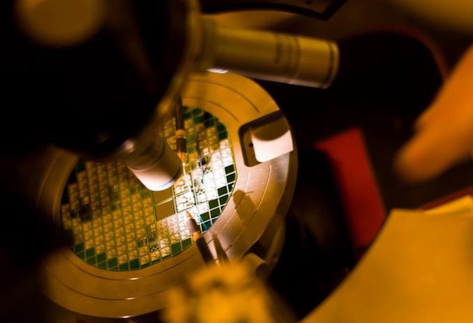
GlobalFoundries and SiFive announced on Tuesday that they will be co-developing an implementation of HBM2E memory for GloFo's 12LP and 12LP+ FinFET process technologies. The IP package will enable SoC designers to quickly integrate HBM2E support into designs for chips that need significant amounts of bandwidth.
The HBM2E implementation by GlobalFoundries and SiFive includes the 2.5D packaging (interposer) designed by GF, with the HBM2E interface developed by SiFive. In addition to HBM2E technology, licensees of SiFive also gain access to the company’s RISC-V portfolio and DesignShare IP ecosystem for GlobalFoundries’ 12LP/12LP+, which will enable SoC developers to build RISC-V-based devices GloFo's advanced fab technology.
GlobalFoundries and SiFive suggest that the 12LP+ manufacturing process and the HBM2E implementation will be primarily used for artificial intelligence training and inference applications for edge computing, with vendors looking to optimize for TOPS-per-milliwatt performance.
For GlobalFoundries, it is important to land customers who need specialized process technologies and may not be ready for leading-edge processes from TSMC and Samsung Foundry for cost or other reasons. As for SiFive's involvement, this is a bit trickier – RISC-V itself isn't likely to be used for the core logic in deep learning accelerators, but it is a solid architecture to use for the embedded CPU cores needed to control the dataflows within an accelerator.
SiFive’s HBM2E interface and custom IP for GlobalFoundries’ 12LP and 12LP+ technology are being developed at GF’s Fab 8 in Malta, New York. The two companies expect that they'll be able to wrap up their work in the first half of 2020, at which point the IP will become available for licensing.
Related Reading:
- GlobalFoundries Unveils 12LP+ Technology: Massive Performance & Power Improvements
- SiFive Announces First RISC-V OoO CPU Core: The U8-Series Processor IP
- Samsung Develops 12-Layer 3D TSV DRAM: Up to 24 GB HBM2
- Samsung HBM2E ‘Flashbolt’ Memory for GPUs: 16 GB Per Stack, 3.2 Gbps
- SK Hynix Announces 3.6 Gbps HBM2E Memory For 2020: 1.8 TB/sec For Next-Gen Accelerators
- SiFive Acquires USB 2.0 and 3.x IP Portfolio to Strengthen RISC-V SoCs
Source: GlobalFoundries


13 Comments
View All Comments
FreckledTrout - Tuesday, November 5, 2019 - link
I wish them all the best. They will be competing with 7nm HBM2E but hey if they can make it cheap enough maybe they will get some takers.PixyMisa - Tuesday, November 5, 2019 - link
AMD's IO dies are produced on GloFo 12nm, so there's potential there.Alexvrb - Tuesday, November 5, 2019 - link
That's an interesting thought. An APU with 12LP+ I/O die and HBM2E, connected to 7nm GPU and CPU chiplets?With that being said, I think AMD's APUs are going to be monolithic with no HBM this time around.
ET - Wednesday, November 6, 2019 - link
AMD can opt for two APU lines, one monolithic for ultraportables and one chiplet based for desktop replacements.Alexvrb - Wednesday, November 6, 2019 - link
It's not worth the (considerable) resources required to create two different designs. We *might* see something like this combined with Zen 3 or later.Xajel - Wednesday, November 6, 2019 - link
But the IO won't stay in 12nm forever, they'll eventually move to 7nm when it becomes mature enough, cheaper enough to make the move worth it, we might see it next year or even the next.Unless, GloFo could find a way to package the HBM with it's interposer with other silicons with much lower cost to make it viable to think about it for APU's
Alexvrb - Wednesday, November 6, 2019 - link
You won't see that happen until their CPU chiplets move to a more advanced node, AND 7nm supply loosens up. The whole point is that the I/O die doesn't scale that well, so instead of wasting wafer space, use a cheaper process. As a result, 12LP+ on GF would be a good choice over the current 12LP, if costs are reasonable.They won't have a choice though with their upcoming APU, since it's likely a monolithic design. But the I/O diespace on such a design will also be considerably less (not to mention other cuts to cache and so forth) so it's probably not a dealbreaker.
deil - Wednesday, November 6, 2019 - link
not everyone need bleeding edge. 12nm is still incredibly powerful and stuff. I expect a lot of mid range snapdragons or mediatek or those kinds of things in there.Alexvrb - Tuesday, November 5, 2019 - link
Their LP+ apparently has pretty substantial gains over 12LP, plus 7nm is both expensive AND supply is tight. All the big players are already gobbling up all the wafers. Designing for 12LP+ is a pretty safe bet as far as costs and wafer supply go.For other specialty designs they've also got 12FDX.
Dragonstongue - Wednesday, November 6, 2019 - link
maybe it is, maybe it is not.just cause it is 7nm does not automatically mean it IS much more pricey, all depends on the foundry (the one who makes it)
if anything, either GloFo will target a more $/unit OR try to be as cost competitive as possible, rarely has it been shown to be BOTH.
I hedge on the latter over the former...time will tell...^.^