GlobalFoundries Unveils 12LP+ Technology: Massive Performance & Power Improvements
by Anton Shilov on September 25, 2019 12:00 PM EST- Posted in
- GlobalFoundries
- Semiconductors
- 14LPP
- 12nm
- 12LP
GlobalFoundries has introduced its 12LP+ fabrication process that relies on the groundwork set by its 14LPP and 12LP technologies and provides significant improvements when it comes to performance, power, and area (PPA) scaling. The specialty foundry positions the technology for developers of chips for cloud and edge AI applications.
GlobalFoundries’ 12LP+ manufacturing technology builds upon the company’s 12LP process yet enables a 20% increase in performance (at the same power and complexity) or a 40% reduction in power requirements (at the same clocks and complexity) as well as a 15% improvement in logic area scaling when compared to 12LP platform. Among other things, 12LP+ supports 0.5V SRAM bit cells (which probably use IP that the company designed for its 7 nm nodes). In addition, GF developed a new 2.5D interposer that enables 12LP+ SoCs to work with HBM memory.
| Advertised PPA Improvements of New Process Technologies Data announced by companies during conference calls, press briefings and in press releases |
||||||
| GlobalFoundries | ||||||
| 12LP+ vs 12LPP |
12LP vs 14LPP |
14HP vs 14LPP |
GF's 7nm Gen 1 vs 14LPP |
|||
| Power | 40% | - | ? | >60% | ||
| Performance | 20% | 10% | ? | >40% | ||
| Area Reduction | 15% | 15% | ? | >50% | ||
The foundry says that its 12LP+ uses a mature design and production ecosystem and provides advantages comparable to those of 7 nm-class fabrication process. Meanwhile, significant improvements and a new PDK point to new design libraries along with numerous new features, which means that GlobalFoundries’ clients will have to make significant investments in order to take advantage of 12LP+. Those investments will still be 50% lower than the cost of transition to a 7 nm-class technology, according to GlobalFoundries.
Michael Mendicino, vice president of Digital Technology Solutions at GF, said the following:
“Our 12LP+ solution already offers clients a majority of the performance and power advantages they would expect to gain from a 7nm process, but their NRE (non-recurring engineering) costs will average only about half as much, a significant savings. Additionally, because the 12 nm node has been running longer and is much more mature, clients will be able to tape-out quickly and take advantage of the growing demand for AI technology.”
To speed up development of 12LP+ chips for its clients, GlobalFoundries has asked Arm to design Arm Artisan physical IP and POP IP required by AI-focused SoCs. That IP is said to be compatible with 12LP. Meanwhile, the 12LP+ PDK is already available and several clients have begun to design chips using the technology. GlobalFoundries expects its customers to tape out the first 12LP+ SoCs sometimes in the second half of 2020 and produce them in volume in 2021.
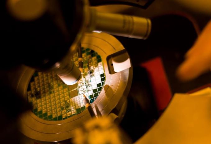
GlobalFoundries will manufacture 12LP+ chips using deep ultraviolet (DUV) lithography with argon fluoride (ArF) excimer lasers operating on a 193 nm wavelength at its Fab 8 in New York, USA. Presumably, the company will use the same equipment that is currently used to make SoCs at 12LP and 14LPP nodes.
Related Reading:
- GlobalFoundries Adds 12LP Process for Mainstream and Automotive Chips; AMD Planning 12LP CPUs & GPUs
- GlobalFoundries Weds FinFET and SOI in 14HP Process Tech for IBM z14 CPUs
- GlobalFoundries Stops All 7nm Development: Opts To Focus on Specialized Processes
- Change of Strategy: A New GlobalFoundries CEO in Dr. Thomas Caulfield
- Samsung Details 11LPP Process Technology: 10 nm BEOL Meets 14 nm Elements
Source: GlobalFoundries


41 Comments
View All Comments
azfacea - Wednesday, September 25, 2019 - link
stolen from TSMCJoeyJoJo123 - Wednesday, September 25, 2019 - link
And they're still on 12nm!!!https://i.imgur.com/lBQ1sxz.gif
levizx - Sunday, September 29, 2019 - link
Sure, steal SADP and change it completely to LELE GREAT strategydel42sa - Monday, November 4, 2019 - link
12nm EUV ? Coolyeeeeman - Wednesday, September 25, 2019 - link
Great, io die on zen 3 will be 12lp I guesshaukionkannel - Thursday, September 26, 2019 - link
Quite possible! The 7nm still will be quite expensive next year. So Ryzen 4000 series could use 12+ production node to reduce electricity usage a Little bit and we would see 7nm IO chip at 2021 with Ryzen 5000 series, when 7nm most likely is more affordable than now (Also more mature, so better yealds)levizx - Sunday, September 29, 2019 - link
They are already using 12LP (and 14LPP) for IO die AFAIKKevin G - Wednesday, September 25, 2019 - link
This would be an improvement for AMD to migrate their IO die for the Milian generation of Epyc chips. AMD doesn't inherently need to change their IO die for that generation as the platform is staying the same as Rome for one more generation. Migrating the IO die to a slightly modified process would improve power consumption and gives them an opportunity to increase the number of chiplets in the same socket.Interesting note about being able to work with HBM. However, the GPU manufacturers are all seemingly looking at TSMC which would constitute the block of chips leveraging HBM. I can only wonder if there is a switch ASIC or similar still contracted at GF that needs this. Then again, perhaps AMD is planning on coupling HBM to their IO die for a unified L4 cache? 32 GB of low(ish) latency memory at 1.5 TB/s of bandwidth would do wonders for AVX-512 or an on-package GPU.
kpb321 - Wednesday, September 25, 2019 - link
The oddball Intel chip that had an on package AMD gpu with one stack of HBM or even their earlier E-DRAM chips showed the value of lots of bandwidth for the integrated GPU. The IGPU's are largely limited by power consumption and memory bandwidth and ultimately your performance is a result of how much you have of both of those and how efficient you are at using them. A laptop APU with some HBM acting as a cache or even just dedicated video memory would have pretty good performance potential.Kevin G - Wednesday, September 25, 2019 - link
HBM would be great for a laptop but it appears that AMD's future endeavors here are all with TSMC's 7 nm node, not GF's 12 nm production.GF pointed out the HBM support means there should be some customer who wants it but AMD and nVidia are place their next wave of HBM supporting devices on TSMC 7 nm.