Intel Releases Broadwell-U: New SKUs, up to 48 EUs and Iris 6100
by Ian Cutress on January 5, 2015 10:00 AM ESTBroadwell GPU Improvements
The new integrated graphics for Broadwell from Intel in the form of HD 5500, HD 6000 and Iris 6100 open up some very important functionality. DirectX 11.2, OpenGL 4.3 and OpenCL 2.0 are big scoring points, especially OpenCL 2.0 when it comes to graphics compute. This includes features such as shared memory coherency between CPU and GPU to allow transfer of pointer-rich memory structures and ultimately the beginnings of heterogeneous CPU + GPU compute.
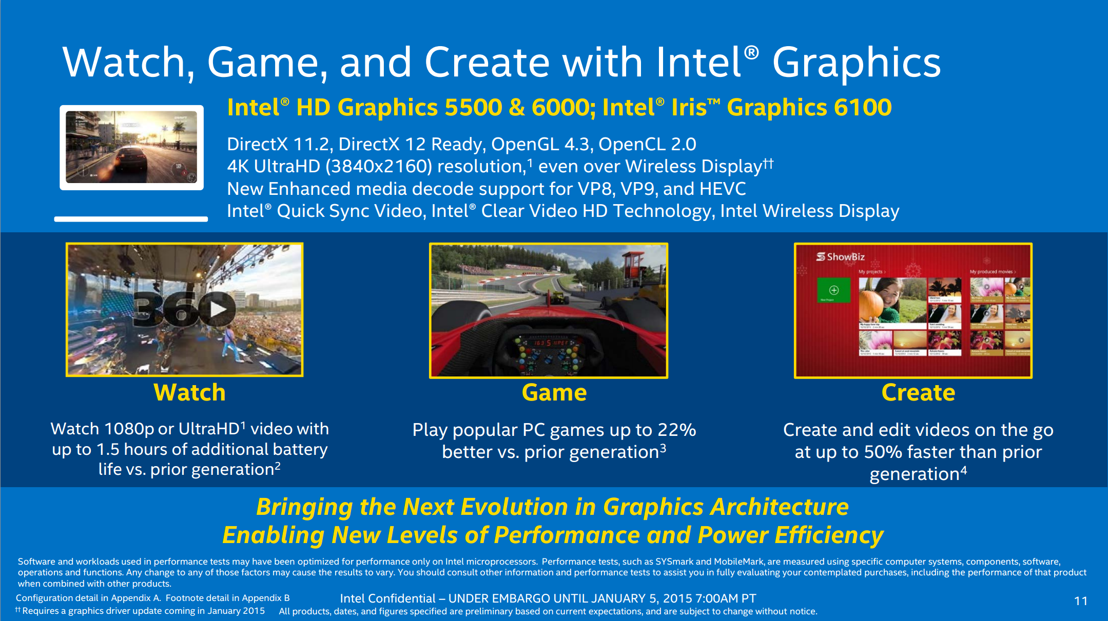
‘DirectX 12 Ready’ is somewhat of an interesting case, and it depends on Microsoft’s final specifications. At this point in time Intel state that they conform to as much of DirectX 12 feature set that they can get their hands on with their relationship with Microsoft, and barring any major addition or change, should be compatible. UHD-4K is also now supported through the HDMI 1.4b interface, albeit limited to 24 Hz.
Support for HEVC is also present in terms of a combined (hybrid) hardware and software solution, just as it was on Core-M. Intel stated that as parts of the H.264 algorithm are near if not identical to those of the H.265, with a small tweak to the hardware it can be used for both. This is still not an all-encompassing hardware acceleration, but it does aim at some parts of the codec. I would speculate that if a full section of the silicon could be made for complete hardware acceleration, it might eat into certain power budgets.
GPU Slices
Although mentioned in our Broadwell architecture overview, for Broadwell-U we should cover the basics of the GPU layout. Below is an image of a HD 6000 implementation featuring two slices of 24 EUs each, with each slice having three sub-slices of 8 EUs. Each EU can handle 7 threads at once when in a 128xSIMD8 32-bit configuration. When in the right data structure, this offers a good amount of power, especially to coalesced 16-bit computation.
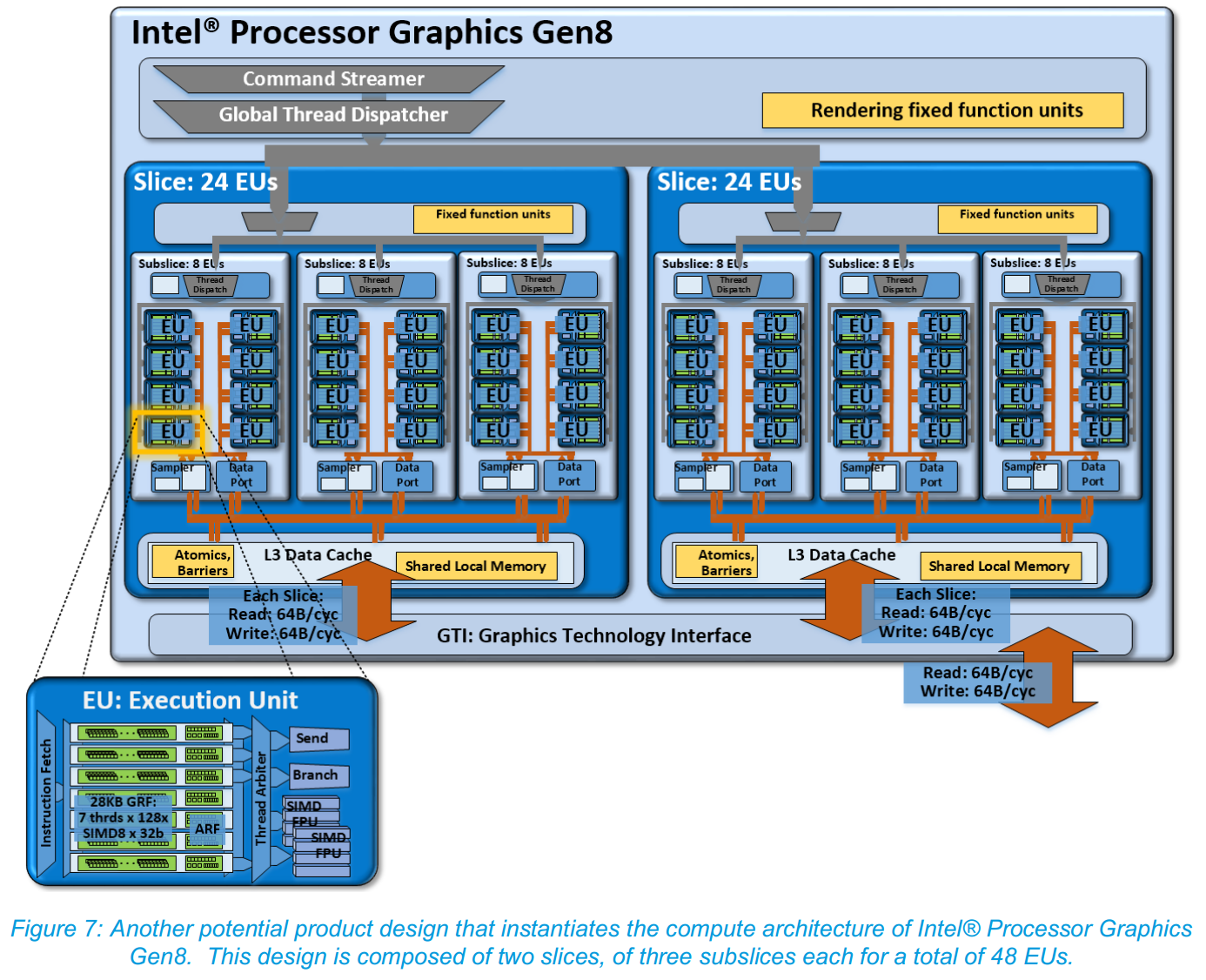
For Broadwell, Intel has reduced the number of EUs in a sub-slice from 10 down to 8. This is a big change, as it eases up the Thread Dispatch, Data Port and L1/L2 samplers in each EU as they have to deal with less data overall. By this logic, with two equivalent designs, one with 8 EUs per sub-slice should be able to get through more data due to less data bandwidth pressure and less competition for each sub-slice’s shared local memory.
Each slice has an L3 Data Cache, which for Gen8 is improved from 384 KB to 576 KB per slice. This ends up being split anyway as 64 KB per sub-slice as shared local memory and 384 KB for inter-slice L3 communication. More slices mean more caching overall, and as an aid to the last level cache outside the GPU, the Graphics Technology Interface has doubled the write bandwidth.

The principle behind caches is to provide a small amount of memory that can be accessed faster at the expense of size. The algorithms in place to predict which data is needed next (or preprogrammed data fetching) helps increase the overall speed of any CPU function, but increasing the size of a cache decreases the need for later caches by reducing the data misses that require trips further out. GPUs are historically bandwidth starved, both for gaming and for compute, so by virtue of having four named caches for the GPU to use and increasing at least the third, this should contribute to the large performance numbers Intel is producing in comparison to the previous generation.
In terms of throughput, Intel gives the following numbers for GT2 / 24 EU configurations:
32b FP: 384 FLOP/cycle = 24 EUs * (2 * SIMD-4 FPU) * (MUL + ADD)
64b DP: 96 FLOP/cycle = 24 EU * SIMD-4 FPU * (MUL + ADD) * 0.5 throughput
32b INT: 192 IOP/cycle = 24 EU * (2 * SIMD-4 FPU) * ADD
The Gen8 EUs will support 16-bit floats (half-floats) natively, as well as 16-bit integers.
We can construct a table calculating out to full performance:
| Intel Gen8 Graphics Throughput | |||
| Processor | 32b FP GFLOPs |
64b DP GFLOPS |
32b INT GFLOPs |
| i7-5557U (48 EUs at 1100 MHz) | 844.8 | 211.2 | 422.4 |
| i5-5257U (48 EUs at 1050 MHz) | 806.4 | 201.6 | 403.2 |
| i3-5157U (48 EUs at 1000 MHz) | 768 | 192 | 384 |
| i7-5250U (48 EUs at 950 MHz) | 729.6 | 182.4 | 364.8 |
| i7-5600U (24 EUs at 950 MHz) | 364.8 | 91.2 | 182.4 |
| i5-5300U (24 EUs a 900 MHz) | 345.6 | 86.4 | 172.8 |
| i3-5010U (23 EUs at 900 MHz) | 331.2 | 82.8 | 165.6 |
| i3-5005U (23 EUs at 850 MHz) | 312.8 | 78.2 | 156.4 |
| Pentium 3805U (12 EUs at 800 MHz) | 153.6 | 38.4 | 76.8 |
Having doubled the EUs not only doubles the performance but the extra bit of frequency also helps.
As we mentioned back in August, the sub-slice also gets some minor improvements to increase pixel and Z-fill rates, and the front end’s geometry units are also beefed up. Further reading can be found on Intel’s PDF on the Gen 8 Graphics Overview from IDF.


85 Comments
View All Comments
Pork@III - Friday, January 16, 2015 - link
Yes with Skylake we have a few new intructions; new memory controller, eDRAM on die area, also few other arcitectural changes. With all these changes together Intel promise significant progress in computational capacity of this generation processors. Intel did not once have promised more than what actually imagined their customers. But we still have hope.jman9295 - Sunday, January 18, 2015 - link
Intel should think about producing a mid-range quad core without HT and without the HD graphics GPU specifically for gaming laptops that come with discrete Nvidia GPUs. Before, it made sense to have the iGPU for non-gaming situations to keep the battery from draining. The laptop would switch back and forth automatically. Now, though, with Maxwell being designed as a mobile architecture from the start, there has to be some way that Nvidia can disable most of the GPU so that it can operate at extremely low power consumption when browsing or doing light tasks. I don't think Intel has ever had a mobile core-i CPU with 4 physical cores and no HT. And I'm pretty sure there never was a mobile core-i CPU that did not have an iGPU. Right now, gamers have the choice of a 4c/8t i7 or a 2c/4t i5 or i7 and nothing in between. Giving us a 4c/4t i5 would bring the cost of halfway decent gaming laptops down to under $1,000 depending on the GPU installed. I'm sure there are plenty of other applications for a mobile CPU like this other than gaming, but this would be the ideal gaming laptop CPU.tipoo - Sunday, January 18, 2015 - link
Why does each EU handle 7 threads, when they have 8 "shaders" each?tipoo - Sunday, January 18, 2015 - link
I have the Iris Pro 5200, I'll be interested to see where that 6100 falls in comparison to it. More EUs, and the other benefits to the small GPU-level caches, but no eDRAM. I think the 5200 should still beat it, but I wonder how close it can come without eDRAM.boe - Wednesday, February 4, 2015 - link
I'd certainly like to know more about the onboard GPU for HTPCs. Will it support 4K@60? 4K 3D specs etc.