Intel Xeon E5-2697 v2 and Xeon E5-2687W v2 Review: 12 and 8 Cores
by Ian Cutress on March 17, 2014 11:59 AM EST- Posted in
- CPUs
- Intel
- Xeon
- Enterprise
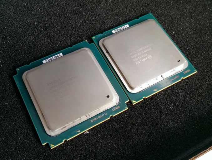
Intel’s roadmap goes through all the power and market segments, from ultra-low-power, smartphones, tablets, notebooks, desktops, mainstream desktops, enthusiast desktops and enterprise. Enterprise differs from the rest of the market, requiring absolute stability, uptime and support should anything go wrong. High-end enterprise CPUs are therefore expensive, and because buyers are willing to pay top dollar for the best, Intel can push core counts, frequency and thus price much higher than in the consumer space. Today we look at two CPUs from this segment – the twelve core Xeon E5-2697 v2 and the eight core Xeon E5-2687W v2.
Firstly I would like to say a big thank you to GIGABYTE Server for the opportunity to test these CPUs in their motherboard, the GA-6PXSV3. This motherboard is the focus of a review at a later date.
Intel’s Enterprise Line
High-end enthusiasts always want hardware to be faster, more powerful, and contain more cores than what is available on the market today. The problem here is two-fold: cost and volume. Were Intel to produce a product for the consumer market at more than $1000, a large part of the market would complain that the ultra-high-end is too expensive. The other issue is volume – it can be hard to gauge just how many CPUs would be sold. For example, the consumer level i7-4930K was the preferred choice for many enthusiasts as it was several hundred dollars cheaper than the i7-4960X despite being a fraction slower at stock frequencies. The ultra-high-end enthusiast also wants all the bells and whistles, such as overclockability, a good range of DRAM speed support and top quality construction materials.
At some point, Intel has to draw the line. The enterprise line of CPUs is different to the consumer in more ways than we might imagine. Due to the requirements of stability, overclocking is knocked on the head for all modern Intel Xeon CPUs. For clarification, the Westmere-EX CPU line (Xeon X5760 et al., socket 1366) was the last line of overclockable Xeons. The Xeon line of CPUs must also support enterprise level memory – UDIMMs and RDIMMs, ECC and non-ECC. This leads up to quad-rank DRAM support, such as 32GB modules that themselves can cost more than a CPU.
Some enterprise CPUs are also designed to speak to other CPUs in multiprocessor systems. On the Intel side, this means a point-to-point QPI link between each CPU in the system. Johan and I have recently tested several multiprocessor systems [1,2,3,4] and as such these features develop over time, cost R&D, and are focused purely on the enterprise sector.
Virtualization is also another feature Intel limits to certain CPUs, although both some consumer and some enterprise Xeons have them. The defining counterpart tends to be overclockability – if a consumer CPU is listed as overclockable, it does not have VT-d extensions for directed I/O. For users that want ECC memory and virtualization at a lower cost, the enterprise product stack often offers lower core/lower frequency parts at lower price points.
While not necessarily verifiable, there have been reports that Xeon processors are actually the better quality samples that come from the fabs. These are CPUs that have better frequency-to-voltage characteristics and have better chance of running cooler. The main reason this report exists is that when Xeons were overclockable back in Westmere, they were more likely to overclock further than the consumer versions. Also it would make sense from Intel’s point of view – the enterprise customer is paying more for their hardware, and as such a better product in terms of energy consumption or thermals would keep those customers happy.
The Xeon Product Line
Intel splits the naming of its Xeons up according to feature set and architecture. For single processor systems using the LGA1150 socket, we get the E3 line of Xeons which at this present time are based on the Haswell architecture and all come under the E3-12xx v3 line:
| Intel E3 v3 SKUs | |||||||
| Xeon E3 v3 | Cores | TDP (W) | IGP | Base Clock | Turbo Clock | L3 Cache | Price |
| E3-1220L v3 | 2/4 | 13 | N/A | 1100 | 1500 | 4 MB | $193 |
| E3-1220 v3 | 4/4 | 80 | N/A | 3100 | 3500 | 8 MB | $193 |
| E3-1225 v3 | 4/4 | 84 | P4600 | 3200 | 3600 | 8 MB | $213 |
| E3-1230 v3 | 4/8 | 80 | N/A | 3300 | 3700 | 8 MB | $240 |
| E3-1240 v3 | 4/8 | 80 | N/A | 3400 | 3800 | 8 MB | $262 |
| E3-1245 v3 | 4/8 | 84 | P4600 | 3400 | 3800 | 8 MB | $276 |
| E3-1270 v3 | 4/8 | 80 | N/A | 3500 | 3900 | 8 MB | $328 |
| E3-1275 v3 | 4/8 | 84 | P4600 | 3500 | 3900 | 8 MB | $339 |
| E3-1280 v3 | 4/8 | 82 | N/A | 3600 | 4000 | 8 MB | $612 |
| E3-1285 v3 | 4/8 | 84 | P4700 | 3600 | 4000 | 8 MB | $662 |
| E3-1265L v3 | 4/8 | 45 | HD (Haswell) | 2500 | 3700 | 8 MB | $294 |
| E3-1284L v3 | 4/8 | 47 | Iris Pro 5200 | 1800 | 3200 | 6 MB | N/A |
| E3-1285L v3 | 4/8 | 65 | P4700 | 3100 | 3900 | 8 MB | $774 |
| E3-1230L v3 | 4/8 | 25 | N/A | 1800 | 2800 | 8 MB | $250 |
With Intel’s enthusiast socket, LGA2011, the processors are now split according to their multi-processor capability. Due to the skip-tock cadence of architecture improvements at this level the enthusiast consumer and Xeon line are both one architecture behind the mainstream LGA1150 CPU line. This results in all the LGA2011 Xeons being based on Ivy Bridge-E.
Single processor LGA2011 Xeons are under the title of E5-16xx v2. Dual processor system capable Xeons are E5-26xx v2, and quad processor system capable Xeons are E5-46xx v2. As Johan pointed out in his excellent dive into the improvements over the older architecture, these CPUs come from three die flavors:
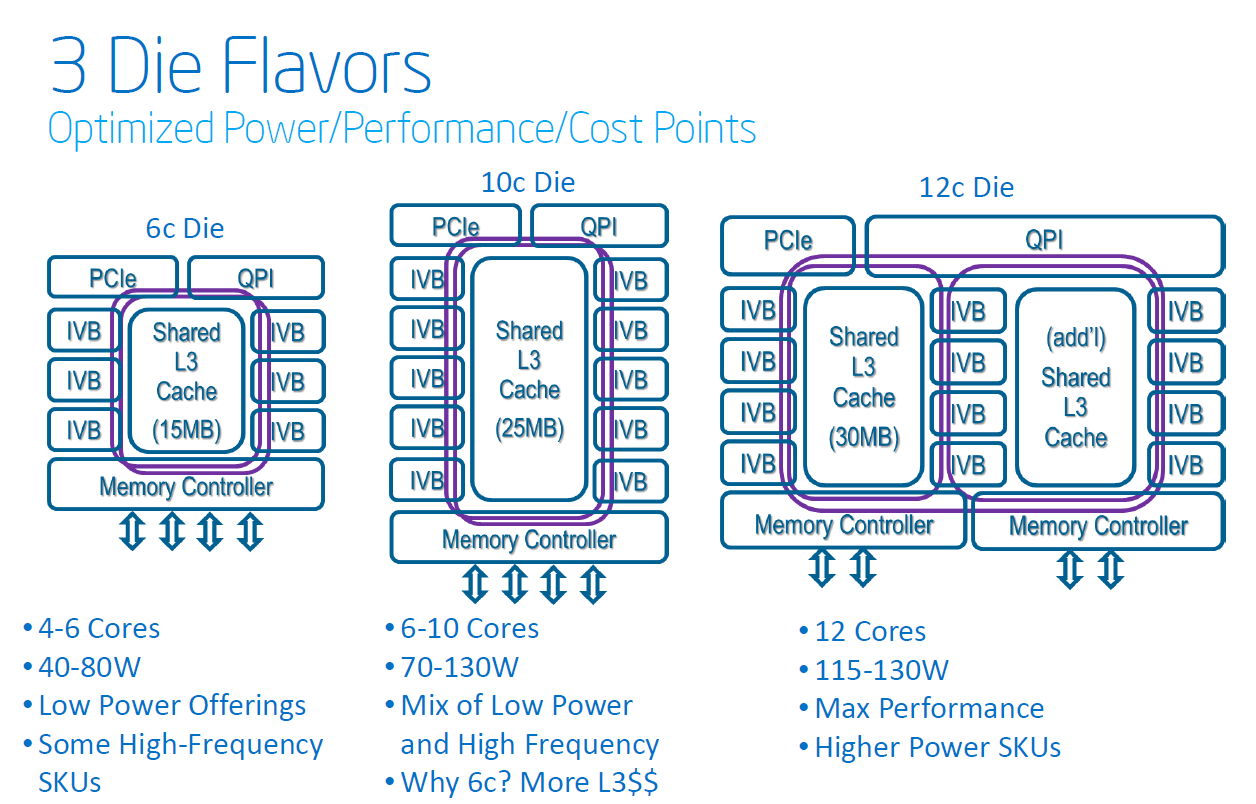
The three dies are aimed at workstations/enthusiasts, servers and high performance computing respectively. I’m not going to repeat what Johan already posted, but it is a really good read if you have a chance to look through it.
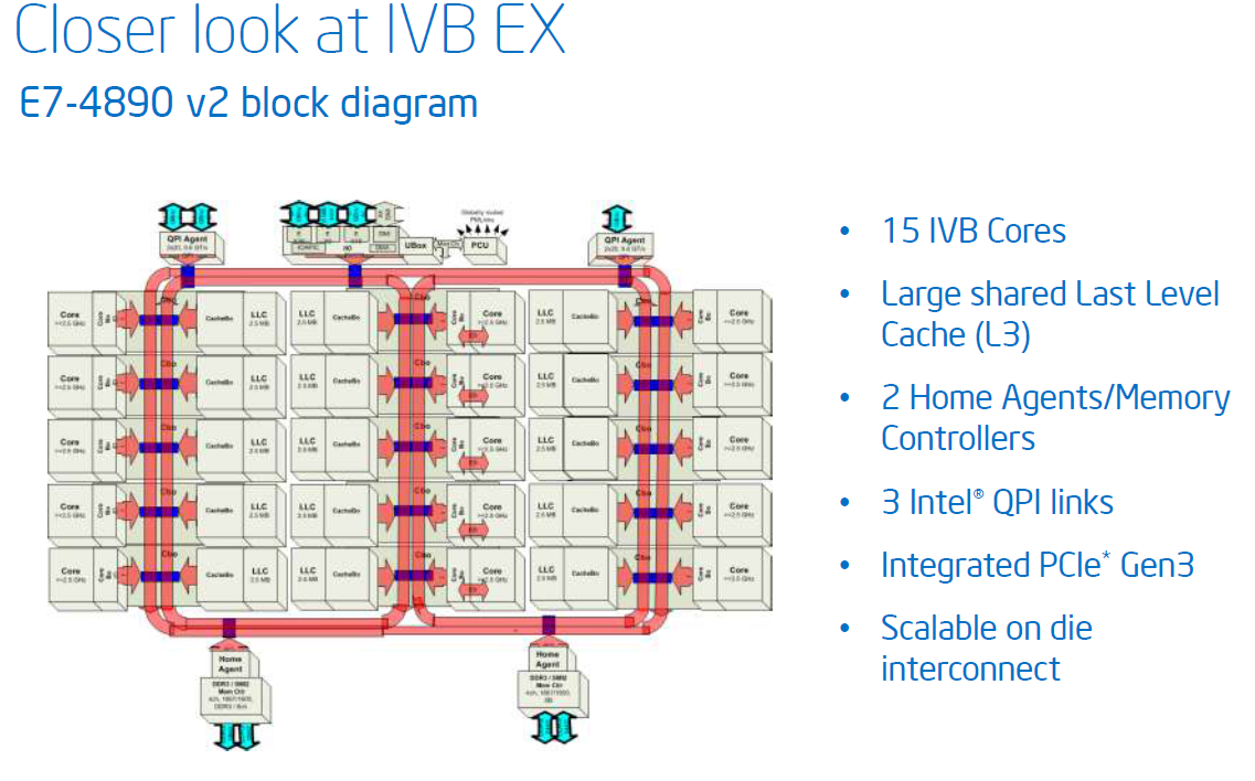
The final batch of processors are in the high performance category, using the LGA2011-1 socket. These have been recently released as the E7 v2 line (again I will point a link to Johan’s deep dive on the specifics) under the Ivy Bridge-EX moniker. We have E7-28xx v2 for 2P, E7-48xx v2 for 4P and E7-88xx v2 for 8P systems. Cores for these CPUs go all the way up to 15 due to the three banks of five used in the die.
Turbo Modes
As with the consumer line, the base clock speed of an enterprise CPU is usually not the be-all and end-all of performance. Intel’s Turbo Boost lets the CPU speed up when fewer cores are in use, exercising the difference in power consumption of one core, two core or all-core computation. There is no hard and fast rule when it comes to the turbo modes – Intel will quote the top turbo bin in its CPU database ark.intel.com but in order to find out the scale of multi-core (but not all-core) operation, one has to look into the specification pdfs, such as this one.
With over 50 different CPUs mentioned in that document, it is hard to see which CPUs are going to offer more than others. We extracted the data:
| Intel E5 SKU Comparison | |||||||
| Xeon E5 | Cores | TDP (W) | Base Clock | Turbo Bins | L3 Cache | L3 Cache / Core | Price |
| E5-46xx | |||||||
| E5-4657L v2 | 12/24 | 115 | 2400 | 5/4/3/3/3/3/3/3/3/3/3/3 | 30 MB | 2.500 | $4,394 |
| E5-4650 v2 | 10/20 | 95 | 2400 | 5/4/3/3/3/3/3/3/3/3 | 25 MB | 2.500 | $3,616 |
| E5-4640 v2 | 10/20 | 95 | 2200 | 5/4/3/3/3/3/3/3/3/3 | 20 MB | 2.000 | $2,725 |
| E5-4624L v2 | 10/20 | 70 | 1900 | 6/6/5/5/4/4/3/3/2/2 | 25 MB | 2.500 | $2,405 |
| E5-4627 v2 | 8/8 | 130 | 3300 | 3/2/2/2/2/2/2/2 | 16 MB | 2.000 | $2,180 |
| E5-4620 v2 | 8/16 | 95 | 2600 | 4/3/2/2/2/2/2/2 | 20 MB | 2.500 | $1,611 |
| E5-4610 v2 | 8/16 | 95 | 2300 | 4/3/2/2/2/2/2/2 | 16 MB | 2.000 | $1,219 |
| E5-4607 v2 | 6/12 | 95 | 2600 | 0/0/0/0/0/0 | 15 MB | 2.500 | $885 |
| E5-4603 v2 | 4/8 | 95 | 2200 | 0/0/0/0 | 10 MB | 2.500 | $551 |
| E5-x6xx | |||||||
| E5-2697 v2 | 12/24 | 130 | 2700 | 8/7/6/5/4/3/3/3/3/3/3/3 | 30 MB | 2.500 | $2,614 |
| E5-2695 v2 | 12/24 | 115 | 2400 | 8/7/6/5/4/4/4/4/4/4/4/4 | 30 MB | 2.500 | $2,336 |
| E5-2687W v2 | 8/16 | 150 | 3400 | 6/5/4/3/2/2/2/2 | 25 MB | 3.125 | $2,108 |
| E5-2667 v2 | 8/16 | 130 | 3300 | 7/6/5/4/3/3/3/3 | 25 MB | 3.125 | $2,057 |
| E5-2690 v2 | 10/20 | 130 | 3000 | 6/5/4/3/3/3/3/3/3/3 | 25 MB | 2.500 | $2,057 |
| E5-2658 v2 | 10/20 | 95 | 2400 | 6/6/5/5/4/4/3/3/2/2 | 25 MB | 2.500 | $1,750 |
| E5-1680 v2 | 8/16 | 130 | 3000 | 9/8/7/5/4/4/4/4 | 25 MB | 3.125 | $1,723 |
| E5-2680 v2 | 10/20 | 115 | 2800 | 8/7/6/5/4/3/3/3/3/3 | 25 MB | 2.500 | $1,723 |
| E5-2643 v2 | 6/12 | 130 | 3500 | 3/2/1/1/1/1 | 25 MB | 4.167 | $1,552 |
| E5-2670 v2 | 10/20 | 115 | 2500 | 8/7/6/5/4/4/4/4/4/4 | 25 MB | 2.500 | $1,552 |
| E5-2648L v2 | 10/20 | 70 | 1900 | 6/6/5/5/4/4/3/3/2/2 | 25 MB | 2.500 | $1,479 |
| E5-2660 v2 | 10/20 | 95 | 2200 | 8/7/6/5/4/4/4/4/4/4 | 25 MB | 2.500 | $1,389 |
| E5-2650L v2 | 10/20 | 70 | 1700 | 4/3/2/2/2/2/2/2/2/2 | 25 MB | 2.500 | $1,219 |
| E5-2628L v2 | 8/16 | 70 | 1900 | 5/5/4/4/3/3/2/2 | 20 MB | 2.500 | $1,216 |
| E5-2650 v2 | 8/16 | 95 | 2600 | 8/7/6/5/5/5/5/5 | 20 MB | 2.500 | $1,166 |
| E5-1660 v2 | 6/12 | 130 | 3700 | 3/2/1/1/1/1 | 15 MB | 2.500 | $1,080 |
| E5-2637 v2 | 4/8 | 130 | 3500 | 3/2/1/1 | 15 MB | 3.750 | $996 |
| E5-2640 v2 | 8/16 | 95 | 2000 | 5/4/3/3/3/3/3/3 | 20 MB | 2.500 | $885 |
| E5-2618L v2 | 6/12 | 50 | 2000 | 0/0/0/0/0/0 | 15 MB | 2.500 | $632 |
| E5-2630 v2 | 6/12 | 80 | 2600 | 5/4/3/3/3/3 | 15 MB | 2.500 | $612 |
| E5-2630L v2 | 6/12 | 60 | 2400 | 4/3/2/2/2/2 | 15 MB | 2.500 | $612 |
| E5-1650 v2 | 6/12 | 130 | 3500 | 4/2/2/2/1/1 | 12 MB | 2.000 | $583 |
| E5-2620 v2 | 6/12 | 80 | 2100 | 5/4/3/3/3/3 | 15 MB | 2.500 | $406 |
| E5-1620 v2 | 4/8 | 130 | 3700 | 2/0/0/0 | 10 MB | 2.500 | $294 |
| E5-2609 v2 | 4/4 | 80 | 2500 | 0/0/0/0 | 10 MB | 2.500 | $294 |
| E5-1607 v2 | 4/4 | 130 | 3000 | 0/0/0/0 | 10 MB | 2.500 | $244 |
| E5-2603 v2 | 4/4 | 80 | 1800 | 0/0/0/0 | 10 MB | 2.500 | $202 |
| E5-x4xx | |||||||
| E5-2470 v2 | 10/20 | 95 | 2400 | 8/7/6/5/4/4/4/4/4/4 | 25 MB | 2.500 | $1,440 |
| E5-2448L v2 | 10/20 | 70 | 1800 | 6/6/5/5/4/4/3/3/2/2 | 25 MB | 2.500 | $1,424 |
| E5-2450L v2 | 10/20 | 60 | 1700 | 4/3/2/2/2/2/2/2/2/2 | 25 MB | 2.500 | $1,219 |
| E5-2450 v2 | 8/16 | 95 | 2500 | 8/7/6/5/4/4/4/4 | 20 MB | 2.500 | $1,107 |
| E5-2428L v2 | 8/16 | 60 | 1800 | 5/5/4/4/3/3/2/2 | 20 MB | 2.500 | $1,013 |
| E5-2440 v2 | 8/16 | 95 | 1900 | 5/4/3/3/3/3/3/3 | 20 MB | 2.500 | $832 |
| E5-2430L v2 | 6/12 | 60 | 2400 | 4/3/2/2/2/2 | 15 MB | 2.500 | $612 |
| E5-2418L v2 | 6/12 | 50 | 2000 | 0/0/0/0 | 15 MB | 2.500 | $607 |
| E5-1428L v2 | 6/12 | 60 | 2200 | 5/4/3/2/2/2 | 15 MB | 2.500 | $474 |
| E5-2420 v2 | 6/12 | 80 | 2200 | 5/4/3/3/3/3 | 15 MB | 2.500 | $406 |
| E5-2407 v2 | 4/4 | 80 | 2400 | 0/0/0/0 | 10 MB | 2.500 | $250 |
| E5-2403 v2 | 4/4 | 80 | 1800 | 0/0/0/0 | 10 MB | 2.500 | $192 |
| Pentium 1405 v2 | 2/2 | 40 | 1400 | 0/0 | 6 MB | 3.000 | $156 |
| E5-1410 v2 | 4/8 | 80 | 2800 | 4/4/3/3 | 10 MB | 2.500 | N/A |
| Pentium 1403 v2 | 2/2 | 80 | 2600 | 0/0 | 6 MB | 3.000 | N/A |
But even this is hard to parse. Some CPUs start off at 3.0 GHz base frequency and have a 900 MHz turbo bin, whereas others move no more than 300 MHz from their base clock. A few CPUs are worthy of attention from our analysis:
The E5-2643 v2 has the most L3 Cache per core of any CPU, at 4.16 MB/core. This is a 10c die offering all 25 MB of L3 cache, but only six cores are active. Reasons for this include database applications that need a large amount of L3 cache per core. For licensing agreements that hinge on per-core pricing, having a larger amount of L3 per core could help save some money by needing fewer cores.
The E5-2667 v2 is a better chip than the E5-2687W v2. The latter gets attention due to its 150W TDP, high base clock and having a ‘W’ in the name. This is partly why I requested it for this review. But the E5-2667 v2 sounds better – a lower TDP (130W vs. 150W), and when you apply all the turbo bins into operation, both CPUs have the same frequency vs. core loading. Both CPUs have a maximum turbo bin of 4.0 GHz, moving down identically to an all-core loading of 3.6 GHz. The E5-2667 v2 is also a cheaper option, and according to the specification sheets can use 768 GB of memory per core, compared to the E5-2687W v2 which can only manage 256 GB.
Low power CPU additions keep their turbo speeds higher for longer. If we look at the turbo bin for a mid-range low power CPU, such as the E5-2628L v2, it goes in pairs: 5/5/4/4/3/3/2/2. The non-low-power processors often end up having a high turbo bin which decreases quickly, such as the E5-2680 v2, which goes 8/7/6/5/4/3/3/3/3.


71 Comments
View All Comments
XZerg - Monday, March 17, 2014 - link
this bench also shows that the haswell had almost no CPU related performance benefits over IVB (if not slowed down performance) looking at 3770k vs 4770k and that haswell ups the gpu performance only.i really question intel's skuing of haswell...
Nintendo Maniac 64 - Monday, March 17, 2014 - link
Emulation?BMNify - Monday, March 17, 2014 - link
its a shame they didn't do a UHD x264 encode here as that would have shown a haswell AVX2 improvement (something like 90% over AVX), and why people will have to wait for the xeons to catch up to at least AVX2 if not AVX3.1psyq321 - Wednesday, March 19, 2014 - link
There is no "90% speedup over AVX" between HSW and IVB architectures.AVX (v1) is floating point only and thus was useless for x264. For floating point workloads you would be very lucky to get 10% improvement by jumping to AVX2. The only difference between AVX and AVX2 for floating point is the FMA instruction and gather, but gather is done in microcode for Haswell, so it is not actually much faster than manually gathering data.
Now, x264 AVX2 is a big improvement because it is an integer workload, and with AVX (v1) you could not do that. So x264 is jumping from SSE4.x to AVX2, which is a huge jump and it allows much more efficient processing.
For integer workloads that can be optimized so that you load and process eight 32-bit values at once, AVX2 Xeon EPs/EXs will be a big thing. Unfortunately, this is not so easy to do for a general-purpose algorithms. x264 team did the great job, but I doubt you will be using 14 core single Haswell EP (or 28 core dual CPU) for H.264 transcoding. This job can be done probably much more efficient with dedicated accelerators.
As for the scientific applications, they already benefit from AVX v1 for floating point workloads. AVX2 in Haswell is just a stop-gap as the gather is microcoded, but getting code ready for hardware gather in the future uArch is definitely a good way to go.
Finally, when Skylake arrives with AVX 3.1, this will be the next big jump after AVX (v1) for scientific / floating point use cases.
Kevin G - Monday, March 17, 2014 - link
Shouldn't both the Xeon E5-2687W v2 support 384 GB of memory? 4 channels * 3 slots per channel * 32 GB DIMM per slot? (Presumably it could be twice that using eight rank 64 GB DIMMs but I'm not sure if Intel has validated them on the 6 and 10 core dies.) Registered memory has to be used for the E6-2687w v2 to get to 256 GB, just is the chip not capable of running a third slots per channel? Seems like a weird handicap. I can only imagine this being more of a design guideline rule than anything explicit. The 150W CPU's are workstation focused which tend to only have 8 slots maximum.Also a bit weird is the inclusion of the E5-2400 series on the first page's table. While they use the same die, they use a different socket (LGA 1356) with triple memory support and only 24 PCI-e lanes. With the smaller physical area and generally lower TDP's, they're aimed squarely the blade server market. Socket LGA 2011 is far more popular in the workstation and 1U and up servers.
jchernia - Monday, March 17, 2014 - link
A 12 core chip is a server chip - the workstation/PC benchmarks are interesting, but the really interesting benchmarks would be on the server side.Ian Cutress - Monday, March 17, 2014 - link
Johan covered the server side in his article - I link to it many times in the review:http://www.anandtech.com/show/7285/intel-xeon-e5-2...
BMNify - Monday, March 17, 2014 - link
a mass of other's might argue a 12 core/24 thread chip or better is a potential "real-time" UHD x264 encoding machine , its just out of most encoders budgets, so NO SALE....Nintendo Maniac 64 - Monday, March 17, 2014 - link
Uh, where's the test set up for the 7850K?Nintendo Maniac 64 - Monday, March 17, 2014 - link
Also I believe I found a typo:"Haswell provided a significant post to emulator performance"
Shouldn't this say 'boost' rather than 'post'?