Applied Materials
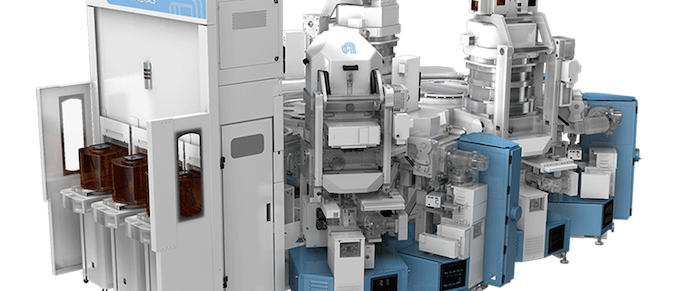
Although the pace of Moore's Law has undeniably slackened in the last decade, transistor density is still increasing with every new process technology. But there is a challenge with feeding power to smaller transistors, as with the smaller transistors comes thinner power wires within the chip, which increases their resistance and may cause yield loss. Looking to combat that effect, this week Applied Materials introduced its new Applied Endura Copper Barrier Seed IMS with Volta Ruthenium Copper Vapor Deposition (CVD) tool, which enables chipmakers to keep using copper for wiring with 2 nm-class and more advanced process technologies. Today's advanced logic processors have about 20 layers of metal, with thin signal wires and thicker power wires. Scaling down wiring with shrinking transistors presents numerous challenges...

Applied Materials Outlines Next-Gen Tools for 3nm and GAA Transistor Era
Last month Samsung Foundry quietly announced that it was set to begin producing chips using its 3GAE (3 nm-class, gate-all-around transistors, early) process technology in the second quarter. While...
17 by Anton Shilov on 5/12/2022
AI Meets Chipmaking: Applied Materials Incorporates AI In Wafer Inspection Process
Advanced system-on-chip designs are extremely complex in terms of transistor count and are hard to build using the latest fabrication processes. In a bid to make production of next-generation...
11 by Anton Shilov on 3/19/2021


