Chipworks Publishes Samsung Galaxy S6 Teardown
by Joshua Ho on April 3, 2015 6:00 PM EST- Posted in
- Smartphones
- Samsung
- Mobile
- Galaxy S6
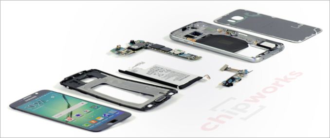
Recently, Chipworks managed to get their hands on the Galaxy S6 and tear down the device to get a closer look at the ICs (integrated circuit) present in the device, which allows for additional analysis of the device. We’re still working on our full review, but we can take a quick look at what Chipworks has found in the device.
This includes an Exynos 7420 SoC that we’ve previously discussed, a Shannon 333 modem along with a Shannon 928 Transceiver and Shannon 710 envelope tracker for the RF front-end. Interestingly, they’ve found an ST-Microelectronics touch controller, which seems to be for the display. Given that most of the Galaxy S and Note family uses Cypress’ CapSense solution for the capacitive touch keys, it’s likely that this is true for the Galaxy S6 as well. Interestingly enough, Chipworks has also identified a Samsung C2N8B6 companion ISP present in the Galaxy S6.

Probably the most interesting aspect of the teardown thus far is that the die size of the 14nm FinFET Exynos 7420 is about 78 mm^2, which is incredibly small compared to the 113 mm^2 size of the 20nm Exynos 5433. It’s unlikely that this is purely due to process as the metal interconnect pitch improvements are relatively minimal when compared to 20nm HKMG, so it’s likely that we’re looking at a great deal of optimization in layout and possibly some IP blocks removed in order to reduce die size. With a die shot floorplan we should be able to figure out exactly what Samsung did to achieve this, and get a good idea of what Samsung has done for the Exynos 7420 which should help with our full review of the Galaxy S6.
Source: Chipworks


47 Comments
View All Comments
FlushedBubblyJock - Friday, April 24, 2015 - link
Amen Solandri - not to mention that metal is very harsh on the hands compared to plastic.But the elitist ego mongers, yeay apple metal..... my GOD how did it ever happen....yeay BROKEN GLASS ON THE BACK !!!
MY GOD THEY ARE RETARDS.
tipoo - Sunday, April 5, 2015 - link
That doesn't even test what the original iPhone bend problem was about. It's testing them both at the middle of the phone. The problems with that iPhone were about the area around the volume keys.tipoo - Saturday, April 4, 2015 - link
Wow, 78mm2 for what is pretty much the new performance champion. I wonder what others who will get more spendy with 14nm die size can accomplish then (Apple perhaps?).PC Perv - Saturday, April 4, 2015 - link
Didn't you previously state how "important" it is to understand that Samsung's 14nm is not "true" 14nm like Intel's? (or TSMC's 16nm for that matter) Because Samsung's 14nm uses the same interconnect as the one used for its 20nm process?It is not the same any more?
tipoo - Sunday, April 5, 2015 - link
That's right. Front-end-of-line process vs Back-end-of-line process. Intel's uses 14nm throughout, including interconnect.PC Perv - Tuesday, April 7, 2015 - link
113mm² to 78mm² can hardly be explained as "20nm with FinFET." Especially not with 2 more GPU clusters.Morawka - Tuesday, April 7, 2015 - link
Chipworks Confirmed that Samsung's 14nm process uses 3D Transistors (finfet)I really hope we get some video cards out on this now that we have a Foundry for hire that can do High Performance Chips at a more advanced lithography process.