Intel at ISSCC 2015: Reaping the Benefits of 14nm and Going Beyond 10nm
by Ian Cutress on February 22, 2015 3:00 PM EST
As part of the International Solid-State Circuits Conference every year, Intel brings forward a number of presentations regarding its internal research. The theme this year at ISSCC is ‘Silicon Systems – Small Chips for Big Data’, and Intel previewed a number of their presentations with the media and analysts last week before the conference. Hot topics being talked about include developments for 14nm features that could potentially be ported to real world devices, technological developments at 22nm using Tri-Gate CMOS for adaptive, autonomous and resilient systems and also a few quick words regarding 10nm and beyond.
Taking Moore’s Law Beyond 10nm
Part of ISSCC will be a round table with representatives from Intel, Qualcomm, a couple of industry companies and university researches discussing how 10nm will attack Moore’s Law and how it can be extended below to 7nm. The graphs shown at IDF 2014 make their presence again, showing cost per square mm and cost per transistor, courtesy of Mark Bohr (Intel Senior Fellow, Logic Technology Development):
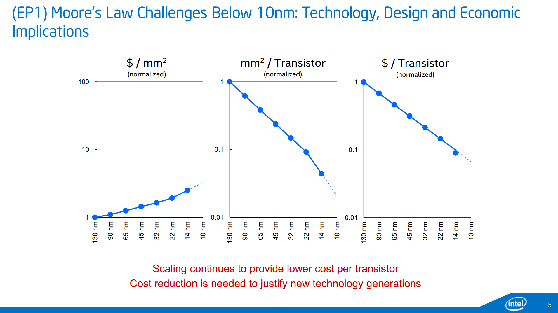
The fact that 14nm resulted in a better-than-the-trend drop in cost per transistor was explained as some internal smart reworking, making sure that certain areas of the dies require different masking and by optimizing the masking process, the cost can be reduced rather than relying on fewer general masks (but it is still a balance).
It was explained that while 10nm will have more masking steps than 14nm, and the delays that bogged down 14nm coming late to market will not be present at 10nm – or at least reduced. We were told that Intel has learned that the increase in development complexity of 14nm required more internal testing stages and masking implementations was a major reason for the delay, as well as requiring sufficient yields to go ahead with the launch. As a result, Intel is improving the efficiency testing at each stage and expediting the transfer of wafers with their testing protocols in order to avoid delays. Intel tells us that that their 10nm pilot lines are operating 50% faster than 14nm was as a result of these adjustments. So while the additional masking steps at 10nm which ultimately increases fixed costs, Intel is still quoting that their methods results in a reducing in terms of cost per transistor without needing a completely new patterning process. EUV lithography was discussed, but Intel seems to be hoping to avoid it until it is absolutely necessary, as EUV development so far has been slower to progress than expected.
10 nm will come with innovation, and getting down to 7 nm will require new materials and processes which Intel wants to promote as a progressive integration between process development and the product design teams. New materials and device structures are key elements on that list, and while III-V materials were discussed in the ISSCC preview, no exact details were given.
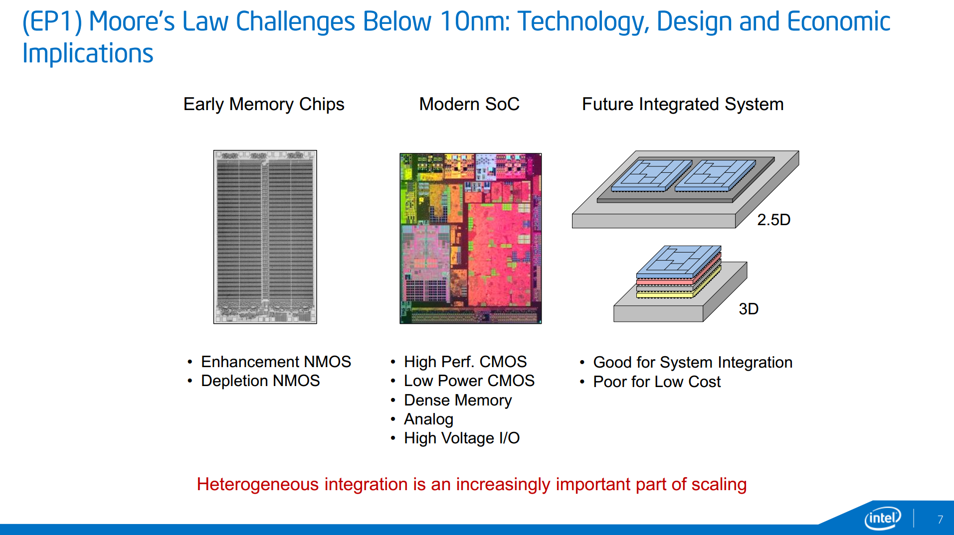
Along with addressing the general challenges in getting down to 7nm, Intel's research group is also looking to address future integrated systems, specifically 2.5D (separate dies on an interposer) and 3D (stacked dies). While 2.5D and 3D are not direct replacements for smaller manufacturing nodes - they just allow you to lay down more transistors at a higher cost - they are being examined as potential solutions for containing power consumption in certian situations (2.5D) or in building better size-limited integrated topologies (3D). Specifically, Intel is looking at scenarios where logic blocks using different fabrication methods are laid out in their own layers and stacked, rather than implemented on a single layer of a single die (think memory, digital logic, and analog communications on a single chip).
These kinds of configuration may appear in smartphones, tablets, or other devices that use highly-integrated chips where multiple types of fabrication would be necessary, and where manufacturers can charge the premium price necessary to cover the additional costs. We have discussed in the past how 2.5D and 3D configurations can improve performance, especially when it comes to memory density and graphics bandwidth, however the price increase (according to Intel) will result in that premium, even at high volume.
Reaping the Benefits of 14nm
Intel is highlighting a trio of papers at ISSCC regarding 14nm. One of the areas ripe for exploitation at 14nm is data transfer, especially transmitters. To that extent, Intel is showing a 14nm Tri-Gate CMOS serializer/deserializer transmitter capable of 16-40 Gbps, using both the NRZ (non-return zero) and PAM4 (Pulse-Amplitude Modulation with 4 levels) modes within a 0.03 millimeter squared die area.
![]()
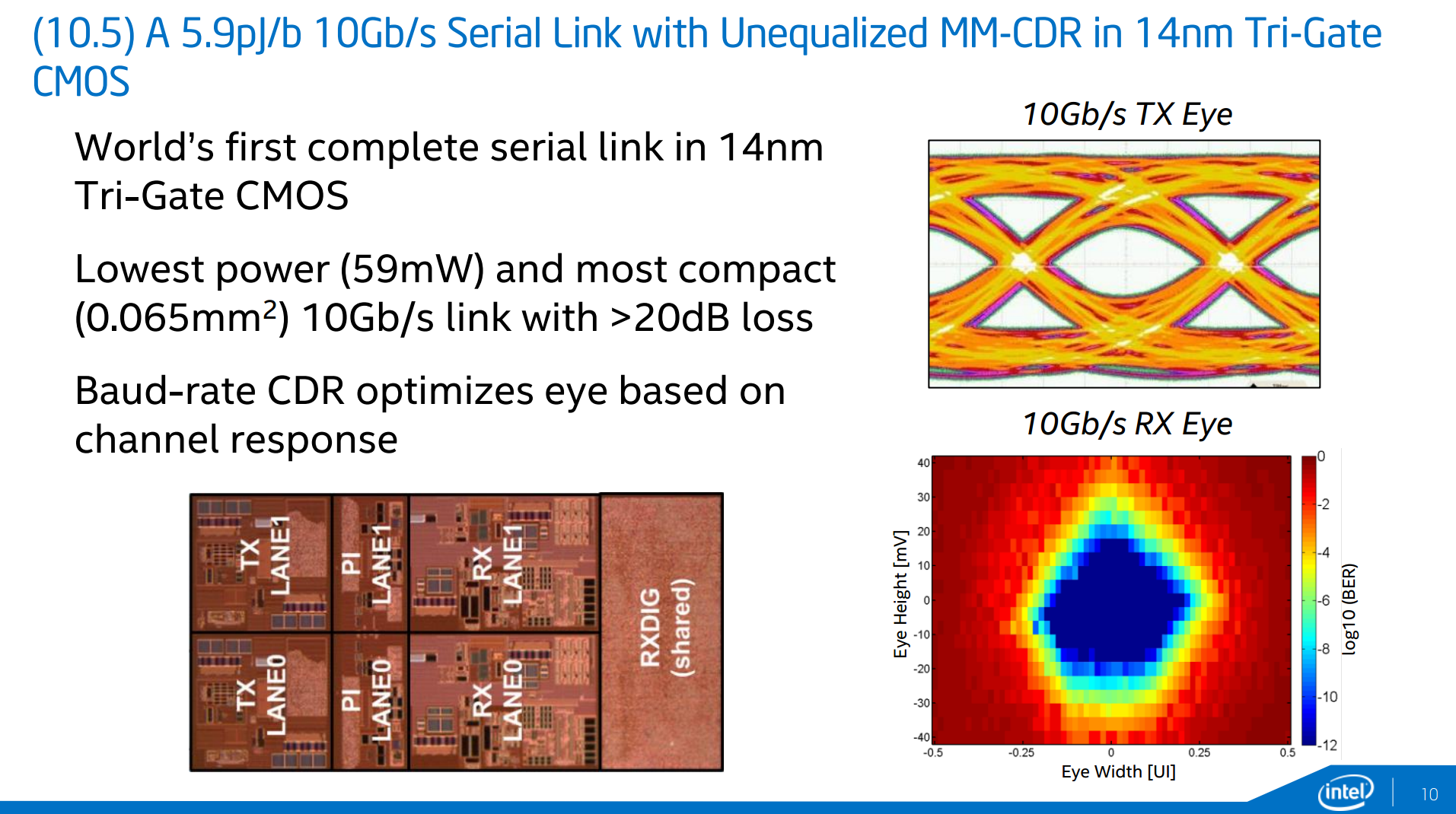
Also on data transfer is a paper regarding the lowest power 10Gb/s serial link and the first complete serial link using 14nm Tri-Gate CMOS. Intel has working silicon at 14nm showing a 59mW power consumption within 0.065 millimeters squared die area that configures the committed data rate to provide the cleanest data response.
Perhaps the most exciting 14nm development is in the form of memory, with Intel describing in-house 84Mb SRAM design that uses the world’s smallest bitcell (0.050 micron squared). At 14nm it represents a doubling of the density at 14.5 Mb per square millimeter, but also provides substantially lower minimum voltage for a given frequency compared to the previous 22nm process. As shown in the graph in the slide, 0.6V is good for 1.5 GHz, but it can scale up to 3 GHz. It is also worth noting that the 14nm yield gradient is more conducive to lower voltage operation compared to the 22nm process. While it seems odd to promote an 84Mb (10.5 MB) design, Intel discussed that it can be scaled up over 100 Mb or more, making it a better solution for embedded devices rather than something like Crystal Well on desktop.

Still Developing on 22nm
While 14nm is great for density, lower voltage and lower power, other features on die are often produced at a looser resolution in order to ensure compatibility but it also offers a great research platform for testing new on-die features to be scaled down at a later date. To this extent, Intel Labs is also presenting a couple of papers about in-house test chips for new features.
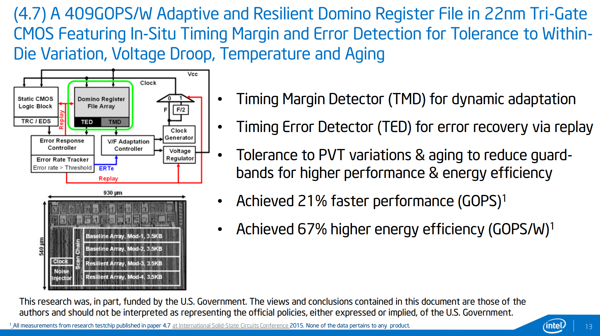
The first test chip concerns data retention within register files. Depending on the external circumstances such as temperature and age, this adaptive and resilient domino register file testchip is designed to realign timing margins and detect errors as they occur and adjust the behavior in order to compensate. The logic that Intel is presenting is designed to also cater for die variation and voltage droop, making it more of a universal solution. On a higher level it sounds like the situation when NAND flash gets old and the onboard controller has to compensate for the voltage level margins.
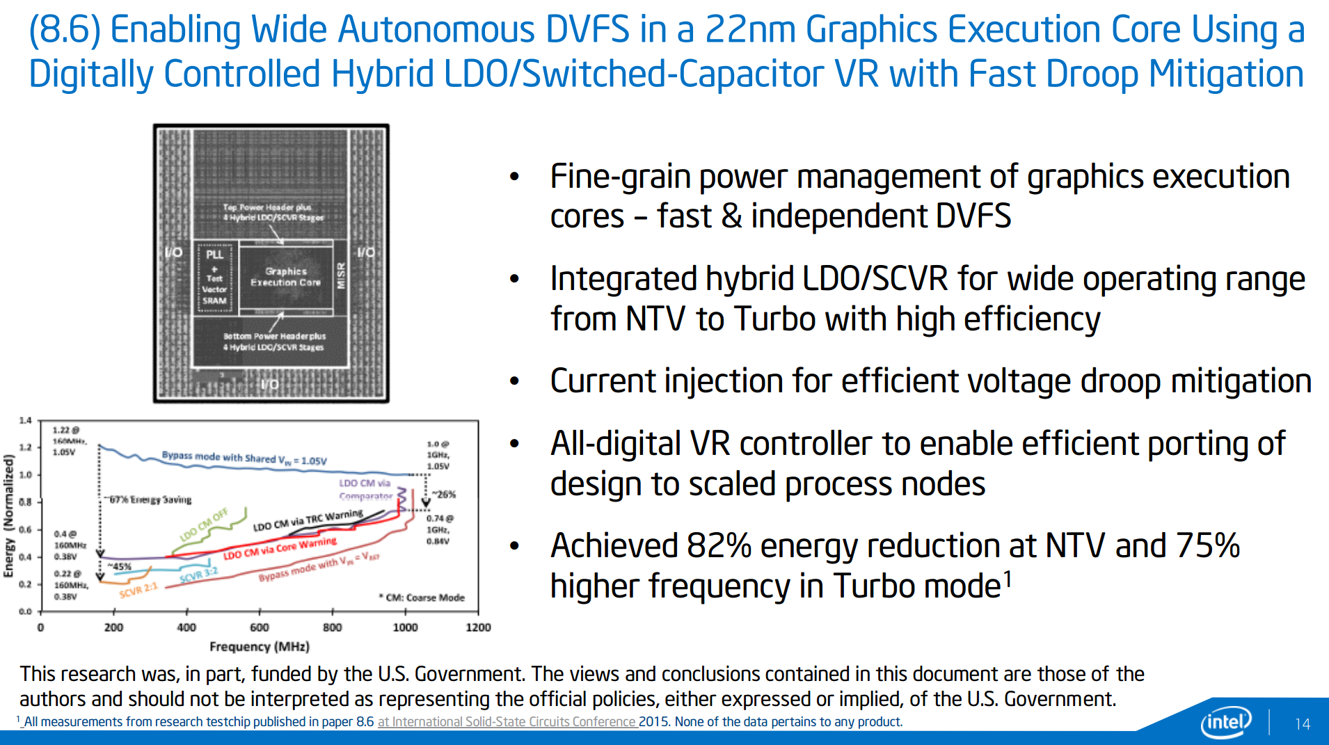
The second test-chip being described brings the situation down to Intel’s execution units in its graphics and dealing with fast, autonomous and independent dynamic voltage scaling. The use of a combined low-dropout regulator (LDO) for low voltages, such as at idle, and a switched capacitor voltage regulator (SCVR) for high voltages allow the appropriate current injection to deal with voltage droop as well as resulting in a large energy reduction. When applied, this should allow for either a power drop at the same frequency, or a higher frequency at the same voltage. Currently the numbers provided by Intel are all on internal silicon rather than anything in the wild, and will be examined at smaller nodes in due course.
Intel at ISSCC
ISSCC always throws out some interesting information about what is actually going on under the hood with the silicon we use almost every day, as we tend to think about it as a black box that slowly gets better over time. In reality, new features are fully researched and documented in order to be included in the next model, as well as trying to keep a balance of power usage and efficiency. On the CPU architecture side of the equation, we reported that Broadwell features needed to show a 2% performance or efficiency improvement for every 1% increase in power, making that advancement steeper than the 1:1 previously required. For all intents and purposes this means that if the same strategy is applied to 10nm and beyond, we are in for a very interesting time. It was interesting to hear about Intel speeding up on 10nm to avoid the delays occurred at 14nm, as well as thoughts regarding future technologies.
The papers Intel is presenting should be available via the ISSCC website as the presentations take place, along with a few others that pique our interest. This should get us ready for some interesting developments come Intel's Developer Forum later in the year.


55 Comments
View All Comments
melgross - Sunday, February 22, 2015 - link
Most chip experts still believe that 5nm may be impossible. I guess we'll just have to wait a good five to seven years to see.witeken - Monday, February 23, 2015 - link
Mark Bohr has recently said that he doesn't see the end of Moore's Law within 10 years (visibility beyond 10 years has always been low). Note that even though the node is called 5nm, most of its feature sizes will be substantially bigger.III-V - Monday, February 23, 2015 - link
Still believe? As of when? It's been generally regarded that we can move past 5nm for a couple of years now.BOMBOVA - Tuesday, February 24, 2015 - link
even though it is far off, say maybe ten years, there is now, some features recognized in nature, that may translate to building 5 nm devices, such as memory cells, gold for example at its smallest scale will make for 5 nm structures, by the simple fact in nature they are bountiful. it is all in assembly now, :) stack my chips, 20 per die, and put lots of light pipes in, Cheers. i am a believer in nature.Samus - Sunday, February 22, 2015 - link
Eventually they will implode :)jjj - Sunday, February 22, 2015 - link
I am more curious about the Marvell presentation:"If chip-design engineers had also looked at the financial optimizations of the overall process, they would have built things differently. They should have realized that certain functions are better grouped into highly specialized integrated circuits that could easily and seamlessly talk to each other without compromising the overall system costs. The key to making this happen is what i call the Lego Block approach of designing integrated circuits. However , in order for the Lego Block approach to materialize, we need to change the way we architect our devices. We need to do many things. Define a new chip-to-chip interconnect protocol , take advantage of multi-chip-module packaging and high-speed SerDes technology ,redefine the memory hierarchy to take advantage of 3D solid-state memory instead of blindly increasing the DRAM size in our devices, repartition DRAM to serve different logical functions instead of building gigantic single-die DRAM to serve every function, change the way we build DRAM,so that they are optimized more for performance and power efficiency instead of capacity and redefine what should be done in hardware versus software. In short, we need to change our way of thinking and be brave enough to reject common wisdom. If we fail to take action, soon we will no longer see cost savings. On the other hand, if we succeed, we willsee life beyond the end of Moore's Law"
Maybe it's too complex to be practical and against the interests of many chipmakers but it is interesting.
No idea if anyone is working on it but i would be curious about the feasibility of a smart interposer where you have "dumb" compute units and memory on an interposer that acts like an interconnect and system agent (as Intel calls the uncore now). So the interposer manages the package and if it was programmable you don't need to fully design it for each specific package, plus you can do software upgrades at any time. Micron's Hybrid Memory Cube is a logic die with dumb DRAM dies stacked on it, a smart interposer would be a somewhat similar concept except the interposer manages the entire system (package).
Unrelated but any clue if anyone is looking into making 3D GPUs? Actual 3D like 3D NAND not chip stacking. Ofc the GPU core is a hell of a lot more complex than a NAND cell but it is a repetitive structure that appears up to a few thousands times on a single die so it kinda makes sense to try to go 3D.
name99 - Monday, February 23, 2015 - link
3D logic is problematic because, while you win on wire length and density, you lose on power dissipation. It's not clear how far you can push it. You MAY be able to get to two layers, if you carefully arrange the lower power blocks (eg memory structures) on top of the higher power blocks (logic), but you may not be able to go further than that.I'm not sure what Marvell is saying that's any different from what, say ARM does today. The most actionable part seems to be a call for more use of specialized DRAMs rather than one single pool of system DRAM. Maybe that makes sense, but it doesn't seem to be a massive change.
antialienado - Sunday, February 22, 2015 - link
I still run on a 45 nm processor, and see no reason for upgrading.Hec. I know people running on 65 nm Quad Core, and there is not enough gain in performance to justify upgrading.
The cost is too high (mother, memory, processor, GPU, power), and the gains negligible.
jjj - Sunday, February 22, 2015 - link
Don't blame it on the process.. What happened is that Intel has no competition and got way greedy. They have smaller and smaller dies despite integrating more and more on the die.Assuming you have a Nehalem , that one was 263 mm^2 and here a die shot where you can see that the cores and the cache are the bulk of the die http://images.anandtech.com/reviews/cpu/intel/neha...
A Haswell based 4770k is 177mm2 and the cores and cache are a much smaller part of the chip http://images.anandtech.com/doci/7003/Screen%20Sho...
We could have 8 cores at reasonable prices,but they make more money by not giving us that since nobody else is actually competing and regulators are sleeping.
voicequal - Sunday, February 22, 2015 - link
Intel has chosen to invest the extra die area into the iGPU and fixed function units like H.264 encode/decode. Arguably these have benefited the mainstream more by eliminating the cost for discrete graphics. For raw CPU/$, the 6-core i7-5820K is nothing to sneeze at. That being said, more competition is rarely bad for the consumer.