Apple A8X’s GPU - GXA6850, Even Better Than I Thought
by Ryan Smith on November 11, 2014 11:00 PM EST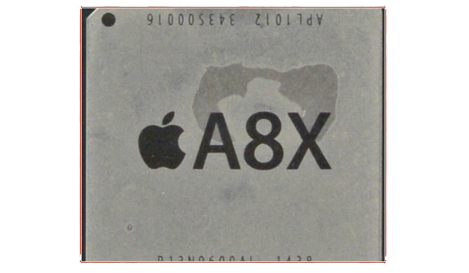
Working on analyzing various Apple SoCs over the years has become a process of delightful frustration. Apple’s SoC development is consistently on the cutting edge, so it’s always great to see something new, but Apple has also developed a love for curveballs. Coupled with their infamous secrecy and general lack of willingness to talk about the fine technical details of some of their products, it’s easy to see how well Apple’s SoCs perform but it is a lot harder to figure out why this is.
Since publishing our initial iPad Air 2 review last week, a few new pieces of information have come in that have changed our perspective on Apple’s latest SoC. As it turns out I was wrong. Powered by what we’re going to call the GXA6850, the A8X’s GPU is even better than I thought.
| Apple SoC Comparison | ||||||
| A8X | A8 | A7 | A6X | |||
| CPU | 3x "Enhanced Cyclone" | 2x "Enhanced Cyclone" | 2x Cyclone | 2x Swift | ||
| CPU Clockspeed | 1.5GHz | 1.4GHz | 1.4GHz (iPad) | 1.3GHz | ||
| GPU | Apple/PVR GXA6850 | PVR GX6450 | PVR G6430 | PVR SGX554 MP4 | ||
| RAM | 2GB | 1GB | 1GB | 1GB | ||
| Memory Bus Width | 128-bit | 64-bit | 64-bit | 128-bit | ||
| Memory Bandwidth | 25.6GB/sec | 12.8GB/sec | 12.8GB/sec | 17.1GB/sec | ||
| L2 Cache | 2MB | 1MB | 1MB | 1MB | ||
| L3 Cache | 4MB | 4MB | 4MB | N/A | ||
| Transistor Count | ~3B | ~2B | >1B | N/A | ||
| Manufacturing Process | TSMC(?) 20nm | TSMC 20nm | Samsung 28nm | Samsung 32nm | ||
Briefly, without a public die shot of A8X we have been left to wander through the dark a bit more than usual on its composition. A8X’s three “Enhanced Cyclone” CPU cores and 2MB of L2 cache were easy enough to discover, as the OS will cheerfully report those facts. However the GPU is more of an enigma since the OS does not report the GPU configuration and performance is a multi-variable equation that is reliant on both GPU clockspeed and GPU width (the number of clusters). Given Apple’s performance claims and our own benchmarks we believed we had sufficient information to identify this as Imagination’s PowerVR GX6650, the largest of Imagination’s GPU designs.
Since then, we have learned a few things that have led us to reevaluate our findings and discover that A8X’s GPU is even more powerful than GX6650. First and foremost, on Monday Imagination announced the PowerVR Series7 GPUs. Though not shipping for another year, we learned from Imagination’s announcement that Series7XT scales up to 16 clusters, twice the number of clusters as Series6XT. This immediately raises a red flag since Imagination never released an 8 cluster design – and indeed is why we believed it was GX6650 in the first place – warranting further investigation. This revelation meant that an 8 cluster design was possible, though by no means assured.
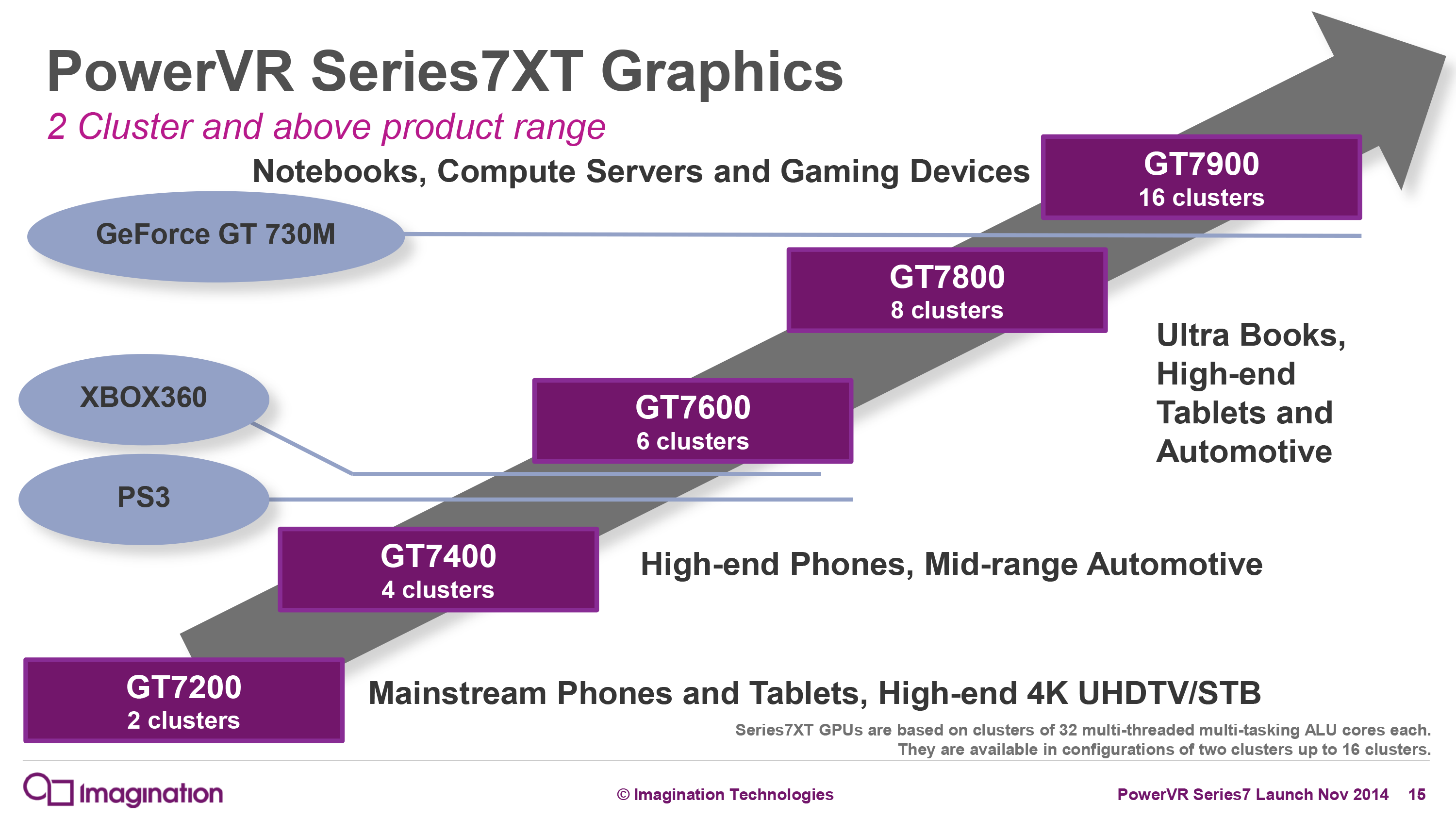
PowerVR Series7XT: Up 16 Clusters, Twice As Many As Series6XT
The second piece of information came from analyzing GFXBench 3.0 data to look for further evidence. While we don’t publish every single GFXBench subtest in our reviews, we still collect the data for Bench and for internal use. What we noticed is that the GFXBench fill rate test is showing more than double the performance of the A8 iPhone 6 Plus. Keeping in mind that performance here is a combination of width and clockspeed, fillrate alone does not prove an 8 cluster design or a 6 cluster design, only that the combination of width and clockspeeds leads to a certain level of performance. In other words, we couldn’t rule out a higher clocked GX6650.
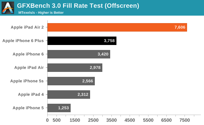
At the same time in the PC space the closest equivalent fillrate test, 3DMark Vantage’s pixel fill test, is known to be constrained by memory bandwidth as much as or more than it is GPU performance (this leading to the GTX 980’s incredible fillrate). However as we have theorized and since checked with other sources, GFXBench 3.0’s fillrate test is not bandwidth limited in the same way, at least not on Apple’s most recent SoCs. Quite possibly due to the 4MB of SRAM that is A7/A8/A8X’s L3 cache, this is a relatively “pure” test of pixel fillrate, meaning we can safely rule out any other effects.
With this in mind, normally Apple has a strong preference for wide-and-slow architectures in their GPUs. High clockspeeds require higher voltages, so going wide and staying with lower clockspeeds allows Apple to conserve power at the cost of some die space. This is the basic principle behind Cyclone and it has been the principle in Apple’s GPU choices as well. Given this, one could reasonably argue that A8X was using an 8 cluster design, but even with this data we were not entirely sure.
The final piece of the puzzle came in this afternoon when after some additional poking around we were provided with a die shot of A8X. Unfortunately at this point we have to stop and clarify that as part of our agreement with our source we are not allowed to publish this die shot. The die shot itself is legitimate, coming from a source capable of providing such die shots, however they didn’t wish to become involved in the analysis of the A8X and as a result we were only allowed to see it so long as we didn’t publish it.
Update: Chipworks has since published their A8X die shot, which we have reproduced below
To get right down to business then, the die shot confirms what we had begun suspecting: that A8X has an 8 cluster Series6XT configuration. All 8 GPU clusters are clearly visible, and perhaps unsurprisingly it looks a lot like the GPU layout of the GX6450. To put it in words, imagine A8’s GX6450 with another GX6450 placed right above it, and that would be the A8X’s 8 cluster GPU.
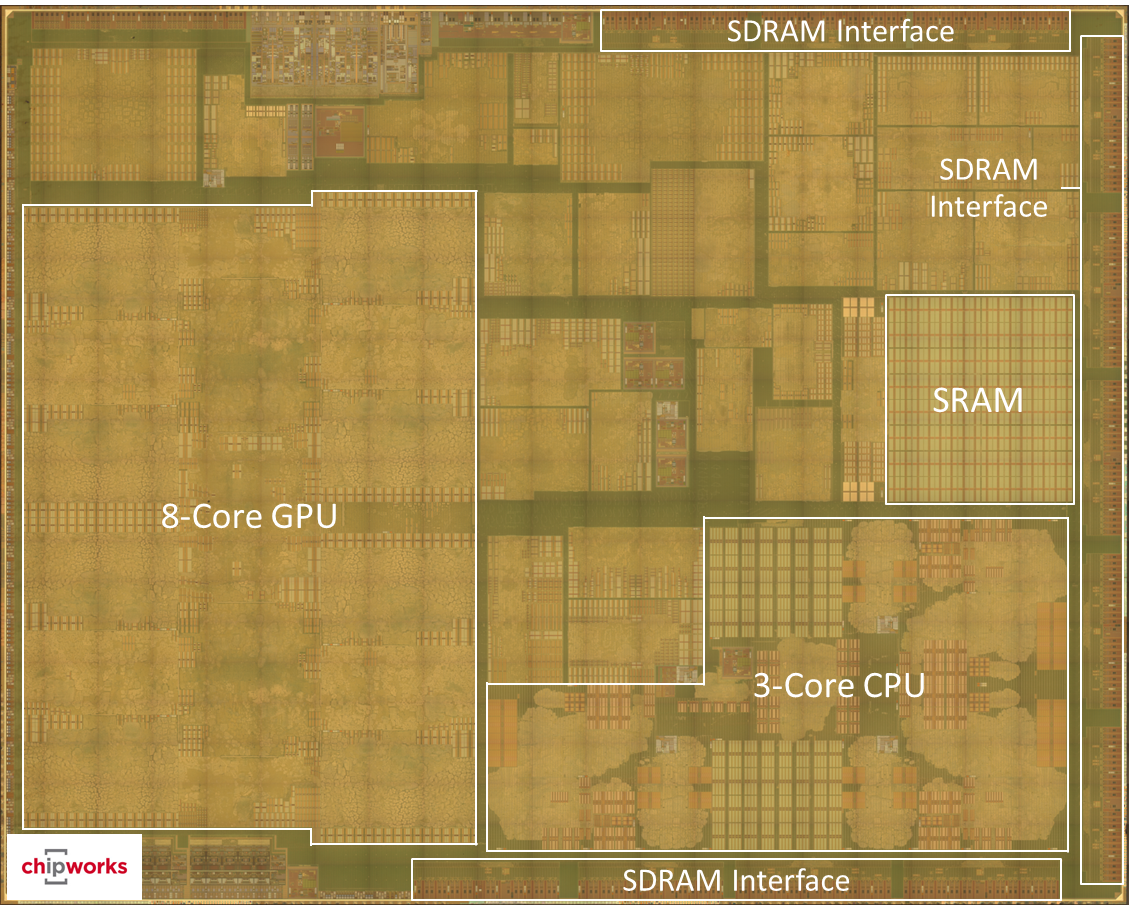
Chipworks A8X Die Shot
With 8 clearly visible GPU clusters, there is no question at this point that A8X is not using a GX6650, but rather something more. And this is perhaps where the most interesting point comes up, due to the fact that Imagination does not have an official 8 cluster Series6XT GPU design. While Apple licenses PowerVR GPU cores, not unlike their ARM IP license they are free to modify the Imagination designs to fit their needs, resulting in an unusual semi-custom aspect to their designs (and explaining what Apple has been doing with so many GPU engineers over the last couple of years). In this case it appears that Apple has taken the GX6450 design and created a new design from it, culminating in an 8 cluster Series6XT design. Officially this design has no public designation – while it’s based on an Imagination design it is not an official Imagination design, and of course Apple doesn’t reveal codenames – but for the sake of simplicity we are calling it the GXA6850.
| Imagination/Apple PowerVR Series6XT GPU Comparison | ||||||
| GXA6850 | GX6650 | GX6450 | GX6250 | |||
| Clusters | 8 | 6 | 4 | 2 | ||
| FP32 ALUs | 256 | 192 | 128 | 64 | ||
| FP32 FLOPs/Clock | 512 | 384 | 256 | 128 | ||
| FP16 FLOPs/Clock | 1024 | 768 | 512 | 256 | ||
| Pixels/Clock (ROPs) | 16 | 12 | 8 | 4 | ||
| Texels/Clock | 16 | 12 | 8 | 4 | ||
| OpenGL ES | 3.1 | 3.1 | 3.1 | 3.1 | ||
Other than essentially doubling up on GX6450s, the GXA6850 appears to be unchanged from the design we saw in the A8. Apple did the necessary interconnect work to make an 8 cluster design functional and made their own power/design optimizations throughout the core, but there do not appear to be any further surprises in this GPU design. So what we have is an Apple variant on a Series6XT design, but something that is clearly a semi-custom Series6XT design and not a full in-house custom GPU design.
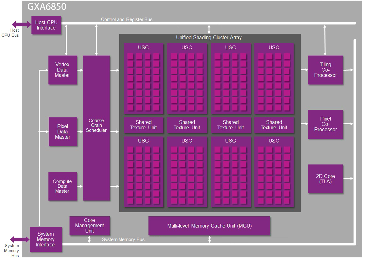
Unofficial GXA6850 Logical Diagram
Meanwhile the die shot places the die size of A8X at roughly 128mm2. This is in-line with our estimates – though certainly on the lower end – making A8X only a hair larger than the 123mm2 A6X. At roughly 3 billion transistors Apple has been able to increase their transistor count by nearly 50% while increasing the die size by only 40%, meaning Apple achieved better than linear scaling and A8X packs a higher average transistor density. On a size basis, A8X is a bit bigger than NVIDIA’s 118mm2 GK107 GPU or a bit smaller than Intel’s 2C+GT2 Haswell CPU, which measures in at 130mm2. Meanwhile on a transistor basis, as expected the 20nm A8X packs a far larger number of transistors than those 28nm/22nm products, with 3B transistors being larger than even Intel’s 4C+GT3 Haswell design (1.7B transistors) and right in between NVIDIA’s GK104 (3.5B) and GK106 (2.5B) GPUs.
| Apple iPad SoC Evolution | |||
| Die Size | Transistors | Process | |
| A5 | 122mm2 | <1B | 45nm |
| A5X | 165mm2 | ? | 45nm |
| A6X | 123mm2 | ? | 32nm |
| A7 | 102mm2 | >1B | 28nm |
| A8X | 128mm2 | ~3B | 20nm |
Of this die space GXA6850 occupies 30% of A8X’s die, putting the GPU size at roughly 38mm2. This isn’t sufficient to infer the GPU transistor count, but in terms of absolute die size it’s still actually quite small thanks to the 20nm process. Roughly speaking an Intel Haswell GT2 GPU is 87mm2, but of course Apple has better density.
Moving on, the bigger question at this point remains why Apple went with an 8 cluster GPU over a 6 cluster GPU. From a performance standpoint this is greatly appreciated, but comparing iPad Air 2 to iPhone 6 Plus, the iPad Air 2 is nowhere near twice as many pixels as the iPhone 6 Plus. So the iPad Air 2 is “overweight” on GPU performance on a per-pixel basis versus its closest phone counterpart, offering roughly 30% better performance per pixel. Apple certainly has gaming ambitions with the iPad Air 2, and this will definitely help with that. But I believe there may also be a technical reason for such a large die.
The 128bit DDR3 memory bus used by the A8X requires pins, quite a lot in fact. Coupled with all of the other pins that need to come off of the SoC – NAND, display, audio, USB, WiFi, etc – and this is a lot of pins in a not very large area of space. At this point I am increasingly suspicious that Apple is pad limited, and that in order to fit a 128bit memory interface A8X needs to reach a minimum die size. With only a small organic substrate to help spread out pads, Apple has only as many pads as they can fit on the die, making a larger die a potential necessity. Ultimately if this were the case, Apple would have some nearly-free die space to spend on additional features if a 6 cluster A8X came in at under 128mm2, making the addition of 2 more clusters (~10mm2) a reasonable choice in this situation.
Finally, while we’re digging around in A8X’s internals, let’s quickly talk about the CPU block. There are no great surprises – nor did we expect to find any – but viewing the A8X die has confirmed that A8X is indeed an asymmetrical 3 CPU core design, and that there is no 4th (disabled) CPU core on the SoC. An odd number of CPU cores is unusual, though by no means unheard of. In this case Apple laid down a 3rd Enhanced Cyclone core, doubled the L2 cache, and left it at that.

Wrapping things up, it has become clear that with A8X Apple has once again thrown us a curveball. By drawing outside of the lines and building an eight cluster GPU configuration where none previously existed, the A8X and its GXA6850 GPU are more powerful than even we first suspected. Apple traditionally aims high with its SoCs, but this ended up being higher still.
As far as performance is concerned this doesn’t change our initial conclusions – iPad Air 2 performs the same no matter how many GPU clusters we think are in it – but it helps to further explain iPad Air 2’s strong GPU performance. With 256 FP32 ALUs Apple has come very close to implementing a low-end desktop class GPU on a tablet SoC, and perhaps just as impressively can sustain that level of performance for hours. Though I don’t want to reduce this to a numbers war between A8X and NVIDIA’s TK1, it’s clear that these two SoCs stand apart from everything else in the tablet space.


114 Comments
View All Comments
chizow - Wednesday, November 12, 2014 - link
Are you being serious here? It would be as if AMD was hypothetically competing with or beating Intel's 22nm chips with their own 28nm chips that used 2/3rd the transistors. The fact they do use a shared fab bodes well for Nvidia because these same avenues for performance gain and power-savings are obviously going to be open to them as well.And what sense would it make for Nvidia to pay the premium that Apple paid to TSMC for early/exclusive access to 20nm when Nvidia does not have nearly the readily available market for their SoC that Apple does? Sure Nvidia is a huge company that primarily makes GPU, but in this arena, they are a small fish compared against the likes of Apple, Samsung, Qualcomm. Apple alone generates some 70-75% of their revenues that number in the tens-of-billions on products that directly rely on their Ax-based SoCs, so of course they are going to spend top dollar to ensure they are on the leading edge of everything. The fact Nvidia is able to even keep up in this regard and even exceed Apple/Qualcomm with <$1Bn in operating budget per year for their Tegra unit is simply amazing, and certainly nothing to be ashamed of.
And what of power consumption? Again they are close enough to the point its really negligible. Nexus 9 has a smaller footprint, smaller battery, slightly better battery life vs. the Ipad Air 2, again taking into consideration Apple's own power-saving claims for A8/A8X this is another amazing accomplishment on the part of Nvidia.
lucam - Wednesday, November 12, 2014 - link
Where did you read about Nexus 9 battery life. I am still waiting for Anand full article.As regards of Nvidia that can't have access to 20nm is just laughable. The soc is not 20nm because at this stage it can't simple as that. If it was Nvidia already started the fabrication of it.
chizow - Wednesday, November 12, 2014 - link
Nexus 9 Battery life is in AT's N9 preview, with iPad Air 2 results and you can see, the N9 edges the Air 2 out with a smaller battery to boot. The Air 2 does have a bigger screen, but you can see, the results are close enough to say battery life/power consumption concerns are negligible between the two.http://images.anandtech.com/graphs/graph8670/68887...
I never said Nvidia wouldn't have access to 20nm eventually, just not in the timeframe slated for Tegra K1. Apple paid for early/exclusive access to it, plain and simple. There was a lot of speculation about this a few years ago and we have seen it come to fruition as Apple is the only SoC maker that is producing 20nm chips from TSMC this year.
http://hothardware.com/Reviews/GameChanger-TSMC-Ma...
At this point there's no reason for Nvidia to go with K1 on 20nm and grow their existing SoC, they'll undoubtedly wait for Erista with Maxwell GPU and increased/refined Denver CPU at this point if they bother to move to 20nm at all.
lucam - Wednesday, November 12, 2014 - link
Do you want really see the battery performance?You will see the Ipad air 2 has longer life and the performance is still the same
http://gfxbench.com/compare.jsp?benchmark=gfx30&am...
Ipad Air 2 long long term: 50.7fps
Nexus 9 long term: 36.6fps
Needless to say those benchmarks are normalised to do a fair comparison.
As I said, Anandtech has to finish his article and you will see they will confirm what found in the gfx bench.
Nvidia can also have access to 20nm when they want, they only need to design a soc that it could fit it.
You then are losing one major point. If Tegra K1 was so efficient, why Nvidia didn't remove some core cpu/gpu to put inside a smartphone? Possibly because they could not reach those level of performance, resulting far behind (maybe) the A7 or Adreno 330.
kron123456789 - Wednesday, November 12, 2014 - link
No, that's because K1 is most simpler Kepler design(1 GPC with 1 SMX). I think they just couldn't remove some of CUDA cores and get it to work. But they can do it with Maxwell because 1 SMM has only 128 CUDA cores and i think they can even split it in two if they want to.chizow - Wednesday, November 12, 2014 - link
Running a benchmark loop is typical usage pattern for most end-users? I think most users would go by a typical light/browser test to see what kind of battery life they get with these devices and as I said, they do show the two are very comparable.Again, Nvidia will go to 20nm or smaller eventually, but that won't happen with Tegra K1, as the process was not available to them. Only Apple had access because they paid for the privilege. If 20nm was an option to Nvidia from the outset for Denver K1, you don't think they would have taken it?
And finally I'm not missing your major point, Tegra K1 would have no problems fitting in a smartphone given it's predecessor Tegra 4 was able to do so, and the K1 has shown to be more power efficient than that. The problem is the lack of integrated LTE which makes it a non-starter for most OEMs/integrators, especially given the fact GPU performance isn't the top driver for smartphone SoC metrics. I guess by the same token the amazing point you are missing is why the A8X isn't in a smartphone?
lucam - Thursday, November 13, 2014 - link
Look Chizow, I showed a benchmark where it was clearly shown the long life battery of Ipad Air 2 vs Nexus 9. Then I showed you also another one where the Ipad Air 2 sustains higher fps during time than Nexus, proving the fact it's more efficient.What else you want me to show, if gfxbench is not enough? You want me to link a naked woman holding an Ipad Air 2 to convince you? What ever I say you find an excuse.
Then you said this no-sense idea that only Apple have access to 20nm. Next year when Apple will move to 16nm, you will same the same.
But the fact is now that the A8X performs better than K1 Denver in any sense, that's it.
Than we got some idiots around that keeps saying that Tegra K1 can be only 1 SMX, so that's why it can't go below that. So why Nvidia didn't improve the old Tegra 4 to put it inside a smartphone? Because they don't have a design for that, and no major vendors want Nvidia inside the smartphone, simple as this!!
Chizow the fact is, to date, there is not Tegra inside the smartphones despite your interesting assumptions; and the K1 is not efficient as A8X.
I wish to find you a link of a nice naked woman with an Ipad Air 2 though!!
deppman - Thursday, November 13, 2014 - link
"Look Chizow, I showed a benchmark where it was clearly shown the long life battery of Ipad Air 2 vs Nexus 9. Then I showed you also another one where the Ipad Air 2 sustains higher fps during time than Nexus, proving the fact it's more efficient"
Eh, but that's not quite right. Here is how the shield long-term performance graph looks: http://images.anandtech.com/doci/8329/Run2FPS.PNG
That's not like many others SoCs (I'm looking at you, Adreno) which throttle in one or two times. That over 100 sustained runs with constant performance. It's only when the Shield gets into battery saving mode when it drops FPS.
The bottom line is until the A8x no other SoC came even close to the K1 in GPU perf/W. And even at 20nm and a huge die, it's arguable if the A8x comes out ahead. 3D mark scores for the Shield Tablet, for example, are 33% higher than the iPad Air 2.
lucam - Friday, November 14, 2014 - link
Take a look at this link:http://gfxbench.com/result.jsp?benchmark=gfx30&...
Shield at 1920x1104 =56.4fps
Ipad Air 2 at 2048x1536 =52.6fps
Google Nexus 9 at 2048x1440 =37.9fps
Xiaomi Mipad at 2048x1536 = 35.9fps
It's obvious that Shield run quicker only because of resolution; if you the other Tegra K1 devices the fps the performance goes down dramatically.
deppman - Saturday, November 15, 2014 - link
That's a link to long-term performance, which favors the devices with better thermal management, and does not support your argument of "only because of the resolution".The Shield and iPad air obviously have better thermal engineering, with the aluminum chassis of the iPad clearly offering the best condition. And if you don't think heat is an issue, consider that the iPad mini 3 doesn't have the A8X.
This link http://gfxbench.com/compare.jsp?benchmark=gfx30&am... is a much more appropriate comparison of relative performance, and your argument is much less convincing, and the K1 has much higher render quality.