The iPad Air Review
by Anand Lal Shimpi on October 29, 2013 9:00 PM ESTAn Update on Apple’s A7: It's Better Than I Thought
When I reviewed the iPhone 5s I didn’t have much time to go in and do the sort of in-depth investigation into Cyclone (Apple’s 64-bit custom ARMv8 core) as I did with Swift (Apple’s custom ARMv7 core from A6) the year before. I had heard rumors that Cyclone was substantially wider than its predecessor but I didn’t really have any proof other than hearsay so I left it out of the article. Instead I surmised in the 5s review that the A7 was likely an evolved Swift core rather than a brand new design, after all - what sense would it make to design a new CPU core and then do it all over again for the next one? It turns out I was quite wrong.
Armed with a bit of custom code and a bunch of low level tests I think I have a far better idea of what Apple’s A7 and Cyclone cores look like now than I did a month ago. I’m still toying with the idea of doing a much deeper investigation into A7, but I wanted to share some of my findings here.
The first task is to understand the width of the machine. With Swift I got lucky in that Apple had left a bunch of public LLVM documentation uncensored, referring to Swift’s 3-wide design. It turns out that although the design might be capable of decoding, issuing and retiring up to three instructions per clock, in most cases it behaved like a 2-wide machine. Mix FP and integer code and you’re looking at a machine that’s more like 1.5 instructions wide. Obviously Swift did very well in the market and its competitors at the time, including Qualcomm’s Krait 300, were similarly capable.
With Cyclone Apple is in a completely different league. As far as I can tell, peak issue width of Cyclone is 6 instructions. That’s at least 2x the width of Swift and Krait, and at best more than 3x the width depending on instruction mix. Limitations on co-issuing FP and integer math have also been lifted as you can run up to four integer adds and two FP adds in parallel. You can also perform up to two loads or stores per clock.
I don’t yet have a good understanding of the number of execution ports and how they’re mapped, but Cyclone appears to be the widest ARM architecture we’ve ever seen at this point. I’m talking wider than Qualcomm’s Krait 400 and even ARM’s Cortex A15.
I did have some low level analysis in the 5s review, where I pointed out the significantly reduced memory latency and increased bandwidth to the A7. It turns out that I was missing a big part of the story back then as well…
A Large System Wide Cache
In our iPhone 5s review I pointed out that the A7 now featured more computational GPU power than the 4th generation iPad. For a device running at 1/8 the resolution of the iPad, the A7’s GPU either meant that Apple had an application that needed tons of GPU performance or it planned on using the A7 in other, higher resolution devices. I speculated it would be the latter, and it turns out that’s indeed the case. For the first time since the iPad 2, Apple once again shares common silicon between the iPhone 5s, iPad Air and iPad mini with Retina Display.
As Brian found out in his investigation after the iPad event last week all three devices use the exact same silicon with the exact same internal model number: S5L8960X. There are no extra cores, no change in GPU configuration and the biggest one: no increase in memory bandwidth.
Previously both the A5X and A6X featured a 128-bit wide memory interface, with half of it seemingly reserved for GPU use exclusively. The non-X parts by comparison only had a 64-bit wide memory interface. The assumption was that a move to such a high resolution display demanded a substantial increase in memory bandwidth. With the A7, Apple takes a step back in memory interface width - so is it enough to hamper the performance of the iPad Air with its 2048 x 1536 display?
The numbers alone tell us the answer is no. In all available graphics benchmarks the iPad Air delivers better performance at its native resolution than the outgoing 4th generation iPad (as you'll soon see). Now many of these benchmarks are bound more by GPU compute rather than memory bandwidth, a side effect of the relative lack of memory bandwidth on modern day mobile platforms. Across the board though I couldn’t find a situation where anything was smoother on the iPad 4 than the iPad Air.
There’s another part of this story. Something I missed in my original A7 analysis. When Chipworks posted a shot of the A7 die many of you correctly identified what appeared to be a 4MB SRAM on the die itself. It's highlighted on the right in the floorplan diagram below:
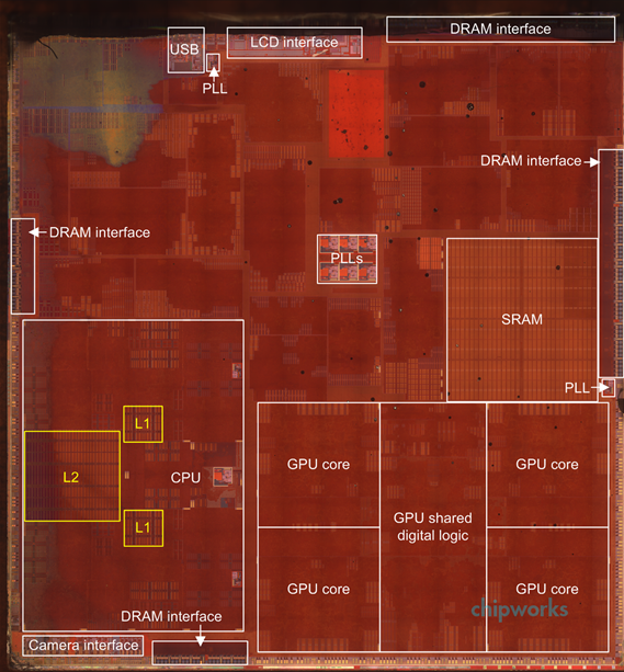
A7 Floorplan, Courtesy Chipworks
While I originally assumed that this SRAM might be reserved for use by the ISP, it turns out that it can do a lot more than that. If we look at memory latency (from the perspective of a single CPU core) vs. transfer size on A7 we notice a very interesting phenomenon between 1MB and 4MB:

That SRAM is indeed some sort of a cache before you get to main memory. It’s not the fastest thing in the world, but it’s appreciably quicker than going all the way out to main memory. Available bandwidth is also pretty good:
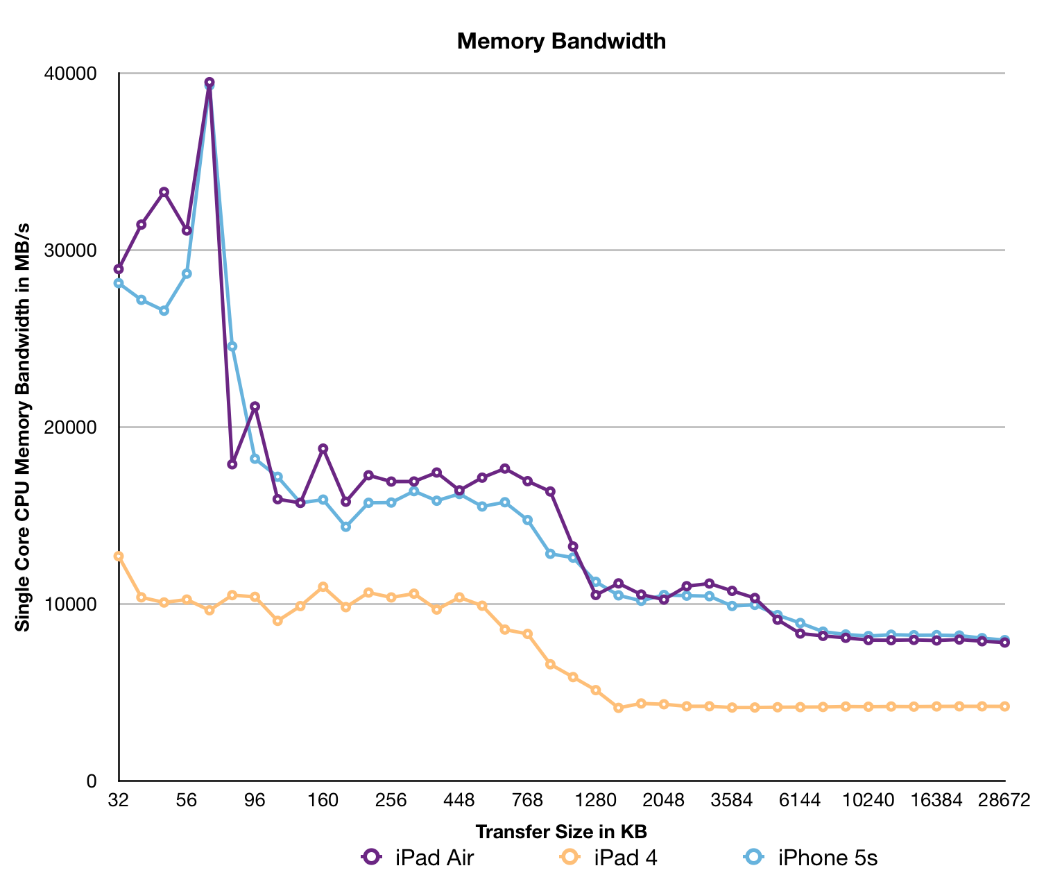
We’re only looking at bandwidth seen by a single CPU core, but even then we’re talking about 10GB/s. Lookups in this third level cache don’t happen in parallel with main memory requests, so the impact on worst case memory latency is additive unfortunately (a tradeoff of speed vs. power).
I don’t yet have the tools needed to measure the impact of this on-die memory on GPU accesses, but in the worst case scenario it’ll help free up more of the memory interface for use by the GPU. It’s more likely that some graphics requests are cached here as well, with intelligent allocation of bandwidth depending on what type of application you’re running.
That’s the other aspect of what makes A7 so very interesting. This is the first Apple SoC that’s able to deliver good amounts of memory bandwidth to all consumers. A single CPU core can use up 8GB/s of bandwidth. I’m still vetting other SoCs, but so far I haven’t come across anyone in the ARM camp that can compete with what Apple has built here. Only Intel is competitive.


444 Comments
View All Comments
Ryan Smith - Wednesday, October 30, 2013 - link
Which is the difference between having me do something, and having Anand do something. There is a very good reason he's The Boss, after all. He's a machine (figuratively speaking).;-)Krysto - Wednesday, October 30, 2013 - link
> A single CPU core can use up 8GB/s of bandwidth. I’m still vetting other SoCs, but so far I haven’t come across anyone in the ARM camp that can compete with what Apple has built here.Didn't Exynos 5250 have 17.5 GB/s bandwidth, according to Samsung's whitepaper? That would be more than 8GB/s per core.
raptorious - Wednesday, October 30, 2013 - link
Maybe if you're talking about L1 or L2 bandwidth, but not DRAM. The DRAM interface on that chip is 2x32 bit and it's clocked at DDR3-1600, which means it can reach a _peak theoretical max_ of 12.8 GB/s. Theoretical bandwidth is one thing, what the CPU can actually sustain to DRAM is a whole different story.AbbyYen - Wednesday, October 30, 2013 - link
the SHIELD is A BEAST!well done NVIDIA, now made it into tablet form with those battery. I don't care if it is a cylinder type, protrude the tablet if you have to so it won't lay flat on table and won't need no magic cover!
iPad for leisure only, play and usefulness is still Android!
darkcrayon - Wednesday, October 30, 2013 - link
Shield is much lower resolution, obviously. Remember also the iPad is (finally) getting official physical controller support, which makes it a potentially much more versatile device than the Shield. And clearly iOS is no slouch when it comes to developer support for games. About the only thing nvidia has here is the willingness to pay for more exclusives. How many people do you think would get a general purpose iPad and use it for awesome games vs buying a one-trick pony like the Shield?ddriver - Wednesday, October 30, 2013 - link
LOL, this is a new high (or low) in manipulative reviews, so now the A7 is faster than a Haswell? With all the money AT pockets in, one would thing they'd at least write a set of in-house REAL CPU benchmarks, especially after all the b1tching about manufacturers cheating in the 3rd party benchmarks that are widely available...Wilco1 - Wednesday, October 30, 2013 - link
It's not as unlikely as you think. An old Cortex-A9 gets half the performance of SB on SPECINT, and A15 is much closer still. Apple's A7 is even wider so should be able to beat a low clocked Haswell. That doesn't mean it can beat the 4GHz beasts - for that Apple would need to clock their A7 much higher and increase core counts, and that is unlikely for now.However I fully agree with you on Anand's state of benchmarks. That he still keeps using SunSpider (one of the most cheated on benchmarks) while at the same time talking about frequency changes as cheating is beyond me. And the claim of A7 being 6-wide is very dubious, it seems to me it's 4-way - it hasn't that much higher IPC than an A15.
thunng8 - Wednesday, October 30, 2013 - link
Not much lower IPC? You've got to be kidding right?A 1.9ghz A15 scores 920 in single core geekbench
A 1.3ghz Apple A7 scores 1400.
IPC looks to be about double on the Apple A7. In what world is double preset close.
Your assertion that deliberately changing frequency when detecting benchmark is not cheating is laughable.
Wilco1 - Wednesday, October 30, 2013 - link
Actually he 64-bit score includes hardware acceleration of crypto functions which artificially inflate the score. The 32-bit integer score is 1065 for 1.3GHz A7 vs 895 for 1.6GHz 5410. That's about 46% IPC gain, or just one generation. A57 will have almost the same IPC as A7, and is still 3-way OoO.Your idea that running a CPU at its designed maximum frequency is cheating is ridiculous. Ever done any benchmarking? I think not. The first thing you do when benchmarking is disable DVFS so you get meaningful and repeatable results at the maximum frequency.
errorr - Wednesday, October 30, 2013 - link
But how does that make benchmarks worthwhile if DVFS is disabled? I want to know if an aggressive throttle is applied in situations. If the DVFS table throttles in the middle of a benchmark the problem is the table.This just shows where ARM needs the most help compared to the other players. Intel and AMD are way ahead in power managment and the newer graphics even throttle much more intelligently, quicker, and with better granularity than any ARM chip. This is one of the last low hanging fruits in performance for such power limited chips. On die voltage regulation is a must for future generations.