A Quick Look at a 22nm Ivy Bridge Wafer
by Anand Lal Shimpi on May 31, 2011 10:42 AM EST- Posted in
- Trade Shows
- CPUs
- Intel
- 22nm
- Ivy Bridge
- Computex 2011
Just before a couple of key Ivy Bridge disclosures, Mooly Eden held up a wafer of 22nm Ivy Bridge CPUs. Presumably these are quad-core versions with 16 EUs, the largest version Intel will make at least at launch. Mooly mentioned that Ivy Bridge will have more than a billion transistors (obviously, SNB was 995M), but he wouldn't reveal the actual count.
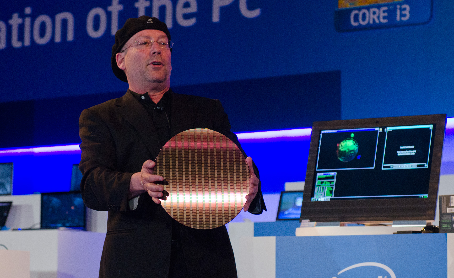
Knowing that these wafers are 300mm in diameter, you should be able to get a decent idea of Ivy Bridge die size based on the photo below.
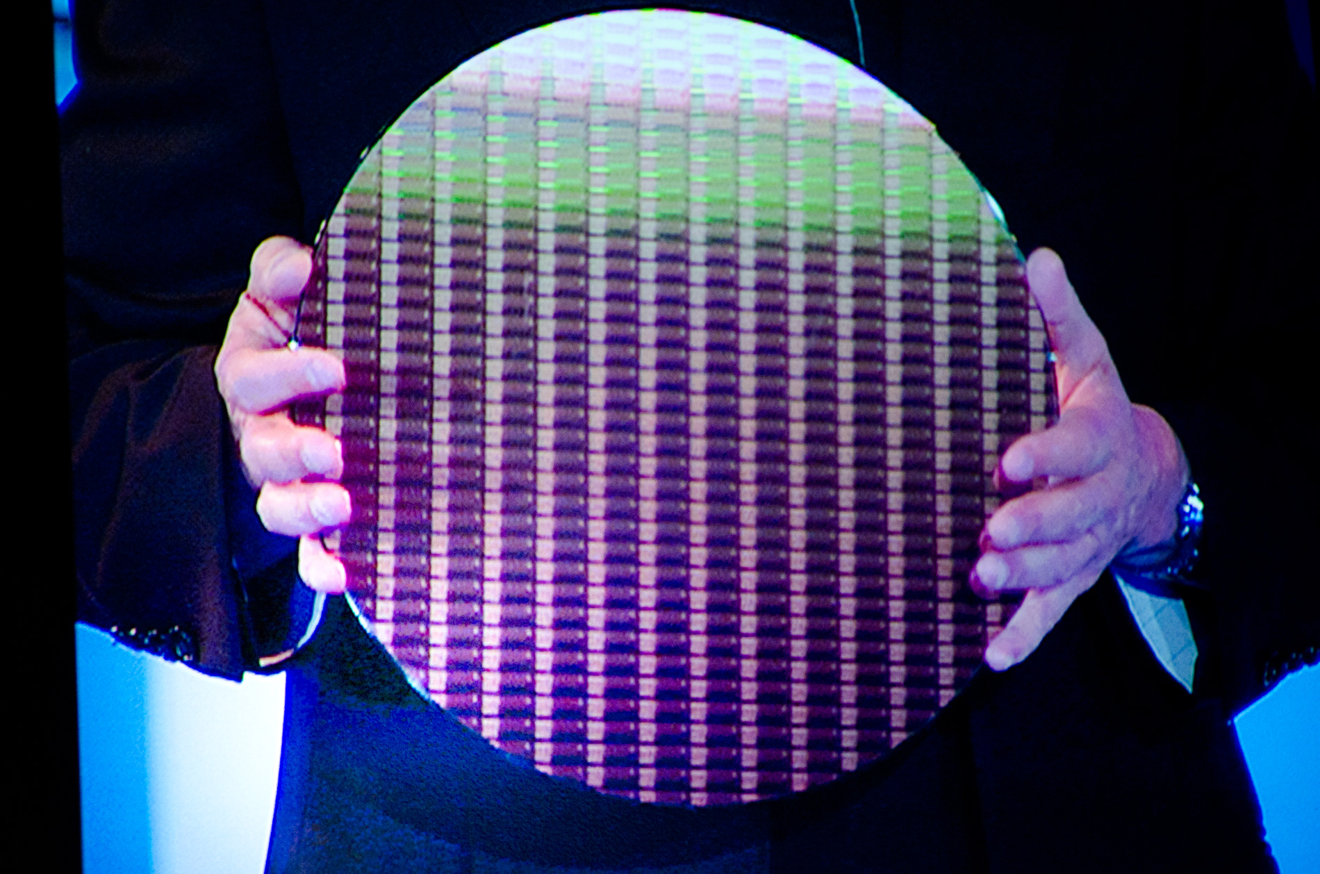
I seem to count approximately 37 die up and 15 die across, which would put a single Ivy Bridge die at 8.1mm x 20mm or around 162mm^2. A 32nm quad-core Sandy Bridge die is 216mm^2 by comparison.


31 Comments
View All Comments
softdrinkviking - Wednesday, June 1, 2011 - link
poor moody! it's just a hat people!i think it's nice. kinda makes him look like a bad-guy in a cyber-punk novel.
TonyB - Tuesday, May 31, 2011 - link
he just needs to grow a mustache and he'll be Jamie Hyneman's twin brother.Jamahl - Tuesday, May 31, 2011 - link
162mm^2 vs 216mm^2, guess what intels priorities are. Not graphics anyway.dananski - Tuesday, May 31, 2011 - link
If you made a SNB with the same number of transistors but at 22nm instead of 32nm, it would be 102mm^2. Ivy bridge seems to have over 50% more area than that, which may well be extra graphics cores among other things :)OneArmedScissorB - Tuesday, May 31, 2011 - link
Somebody should have used a calculator. :pThis is pretty much a straight shrink, with just barely a little extra for the paltry 4 more EUs. There doesn't even appear to be more cache, which raises even more questions about Intel's outlandish claims of a 20% increase in "performance."
DanNeely - Tuesday, May 31, 2011 - link
having a calculator is pointless if you don't put the right stuff into it.. Feature size is related to area, or feature size squared. (22/32)^2 =47%. 216*.47 = 102mm. Jamahl's math is correct. They've got 50% more transistors being used for (mostly undefined) stuff. The extra 4 EUs are part, but unless they got significantly larger most of the extra area is going to something else.maroon1 - Tuesday, May 31, 2011 - link
"This is pretty much a straight shrink, with just barely a little extra for the paltry 4 more EUs"HD2000 which has 6 EU and it is faster than Clarkdale GPU which has 12 EU, and much faster than GMA 4500 which has 10 EU
krumme - Tuesday, May 31, 2011 - link
Now the size is about okey, but should be fun competing with 40mm2 28nm bobcats wether or not AMD and Intel likes it.So next step must be good performance where it matters for the consumer segment. 16 eu and so what?
My SB still have gpu drivers that gives bad performance. All that excellent production technology wasted for nothing.
Doltmoopsie - Tuesday, May 31, 2011 - link
They are going to be selling a 25% smaller die in Ivy Bridge, when compared to Sandy Bridge. Intel should jump to 32 EU's for laptops and full-price desktop parts.Perhaps they can't feed 32 EU's with memory bandwidth, but they should at least give us 24 EU's as was once rumored. When you are at 50% of the performance of a $65 card, you need to CATCH UP not just tread water.
ChuckDriver - Tuesday, May 31, 2011 - link
My guess is that primarily Intel wants more dies per wafer, which should result in greater margin on these products. A secondary reason for Intel "treading water" with the number of execution units, a very apt metaphor, could be the Federal Trade Commission's legal action against Intel. Maybe Intel fears further action if it continues eroding the bottom end of the GPU market with a higher performance solution and it does not want to appear to the FTC as being anticompetitive.