TSMC Outlines Path to EUV Success: More Tools, More Wafers, & Best Pellicles In Industry
by Anton Shilov on May 17, 2024 2:00 PM EST- Posted in
- Semiconductors
- EUV
- ASML
- TSMC
- TSMC Symposium 2024
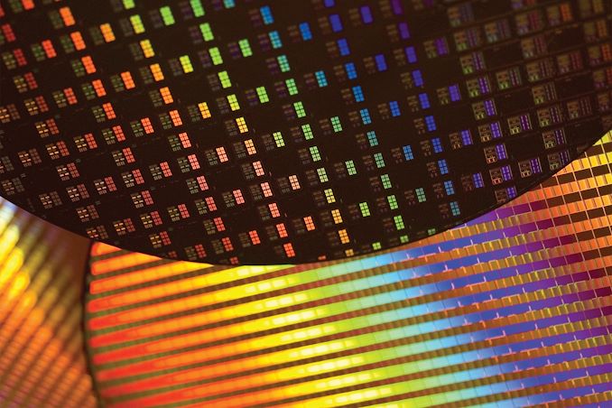
Although TSMC can't claim to be the first fab to use extreme UV (EUV) lithography – that title goes to Samsung – they do get to claim to be the largest. As a result, the company has developed significant experience with EUV over the years, allowing TSMC to refine how they use EUV tooling to both improve productivity/uptime, and to cut down on the costs of using the ultra-fine tools. As part of the company's European Technology Symposium this week, they went into a bit more detail on their EUV usage history, and their progress on further integrating EUV into future process nodes.
When TSMC started making chips using EUV lithography in 2019 on its N7+ process (for Huawei's HiSilicon), it held 42% of the world's installed base of EUV tools, and even as ASML ramped up shipments of EUV scanners in 2020, TSMC's share of EUV installations actually increased to 50%. And jumping ahead to 2024, where the number of EUV litho systems at TSMC has increased by 10-fold from 2019, TSMC is now 56% of the global EUV installed base, despite Samsung and Intel ramping up their own EUV production. Suffice it to say, TSMC made a decision to go in hard on EUV early on, and as a result they still have the lion's share of EUV scanners today.
Notably, TSMC's EUV wafer production has increased by an even larger factor; TSMC now pumps out 30 times as many EUV wafers as they did in 2019. Compared to the mere 10x increase in tools, TSMC's 30x jump in production underscores how TSMC has been able to increase their EUV productivity, reduce service times, and fewer tool downtimes overall. Apparently, this has all been accomplished using the company's in-house developed innovations.
| TSMC's Leadership in EUV High Volume Manufacturing Data by TSMC (Compiled by AnandTech) |
||||
| 2019 | 2023 | |||
| Cumulative Tools | 1X | 10X | ||
| Share of Global EUV Installed Base | 42% | 56% | ||
| EUV Wafer Output | 1X | 30X | ||
| Wafer per Day per EUV Tool | 1X | 2X | ||
| Reticle Particle Contamination | 1X | 0.1X | ||
TSMC says that it has managed to increase wafer-per-day-per-tool productivity of its EUV systems by two times since 2019. To do so, the company optimized the EUV exposure dose and the photoresist it uses. In addition, TSMC greatly refined its pellicles for EUV reticles, which increased their lifespan by four times (i.e., increases uptime), increased output per pellicle by 4.5 times, and lowered defectivity by massive 80 times (i.e., improves productivity and increases uptime). For obvious reasons, TSMC does not disclose how it managed to improve its pellicle technology so significantly, but perhaps over time the company's engineers are going to share this with academia.
| TSMC's EUV Pellicle Technology vs. Commercial Data by TSMC (Compiled by AnandTech) |
||||
| Commercial | TSMC (Claimed) | |||
| Output | 1X | 4.5X | ||
| Defectivity | 1X | 0.0125X | ||
| Lifespan | 1X | 4X | ||
EUV lithography systems are also notorious for their power consumption. So, in addition to improving productivity of EUV tools, the company also managed to reduce the power consumption of its EUV scanners by 24% through undisclosed 'innovative energy saving techniques.' And the company isn't done there: they are planning to improve energy efficiency per wafer per EUV tool by 1.5 times by 2030.
Considering all the refinements that TSMC has managed to achieve with Low-NA EUV lithography by now, it is not terribly surprising that the company is quite confident that it can continue to produce cutting-edge chips in the future. Whereas rival Intel has gone all-in on High-NA EUV for their future, sub-18A nodes, TSMC is looking to leverage their highly-optimized and time-tested Low-NA EUV tooling instead, avoiding the potential pitfalls of a major technology transition so soon while also reaping the cost benefits of using the well-established tooling.
Source: TSMC European Technology Symposium 2024


20 Comments
View All Comments
Papaspud - Sunday, May 19, 2024 - link
It really doesn't matter what Apple wants, there is only 1 High NA machine in the world, and it is just being set up and tested right now- Intel owns it. It is going to be a while-2025? before anything hits the market, and I bet if Apple sees an advantage- they will hire intel to make their chips. Intel wants to be a foundry for hire again, that would be a giant leap...just a thought. ReplyZoolook13 - Sunday, May 19, 2024 - link
Not in 2025, earliest 2026, and TSMC doesn't plan to use HIgh-NA until 2027 or 2028, I'm sure they have the tools when they want them.That everyone is making waves about who takes first delivery of a new machine being put in a lab to develop future tools is pointless, it's the production processes and their characteristics that matter to us consumers in the end.
What's interesting is if one of them are unable to follow their plans.
Btw TSMCs best low-NA scanner allows for better characteristics than the first High-NA machine. Reply
evanh - Monday, May 20, 2024 - link
Intel's outlay in such a small space of time is extraordinary. Some of the machines will end up collecting dust for a while me thinks. ReplyDante Verizon - Sunday, May 19, 2024 - link
Apple is not a foundry, guy. It's up to TSMC, which dominates the sector, to see whether it has an advantage or not. ReplyBlastdoor - Monday, May 20, 2024 - link
https://www.extremetech.com/computing/report-intel...Five or six machines to be delivered in 2024, all to Intel. Reply
evanh - Monday, May 20, 2024 - link
Machine #2 shipped a month back. It went to an unnamed customer in the US. Speculation has it at a research facility that IBM is partnered with. https://www.anandtech.com/show/21356/asml-patterns... Replylefty2 - Sunday, May 19, 2024 - link
The whole point is to reduce costs of producing wafers, not to have the biggest EUV machine from ASML. So, if TSMC can produce wafers overall cheaper with Low NA EUV machines using customised pelliceles and resists, then they will beat Intel. ReplyBlastdoor - Monday, May 20, 2024 - link
I think the whole point for leading edge customers is to increase performance/watt. ReplyAnymoore - Monday, May 20, 2024 - link
The wafers per day was increased by getting higher EUV source power (400W vs. 250W). That's the key advantage over competitors. ReplyAnymoore - Monday, May 20, 2024 - link
This article doesn't tell the whole story.From 2022 to 2023 the wafer output was flat even though EUV tools increased ~30%. N3 appears to have reduced the productivity.
https://semiwiki.com/forum/index.php?threads/intel... Reply