As HPC Chip Sizes Grow, So Does the Need For 1kW+ Chip Cooling
by Anton Shilov on June 27, 2022 10:00 AM EST- Posted in
- Semiconductors
- Immersion
- TSMC
- CoWoS
- 3D Packaging
- 3DFabric
- InFO
One trend in the high performance computing (HPC) space that is becoming increasingly clear is that power consumption per chip and per rack unit is not going to stop with the limits of air cooling. As supercomputers and other high performance systems have already hit – and in some cases exceeded these limits – power requirements and power densities have continued to scale up. And based on the news from TSMC's recent annual technology symposium, we should expect to see this trend continue as TSMC lays the groundwork for even denser chip configurations.
The problem at hand is not a new one: transistor power consumption isn't scaling down nearly as quickly as transistor sizes. And as chipmakers are not about to leave performance on the table (and fail to deliver semi-annual increases for their customers), in the HPC space power per transistor is quickly growing. As an additional wrinkle, chiplets are paving the way towards constructing chips with even more silicon than traditional reticle limits, which is good for performance and latency, but even more problematic for cooling.
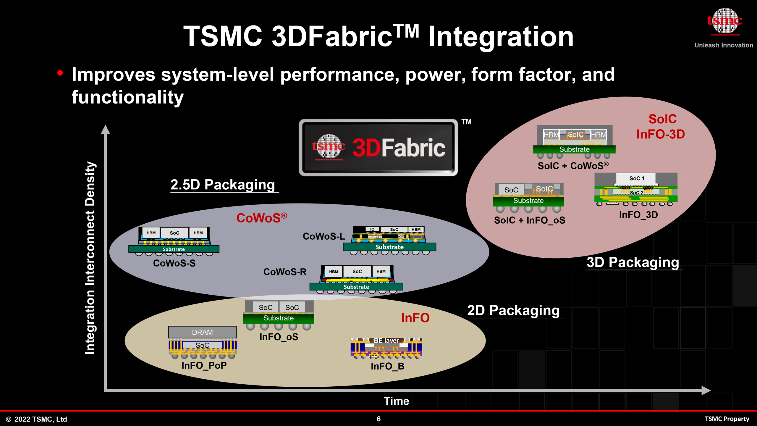
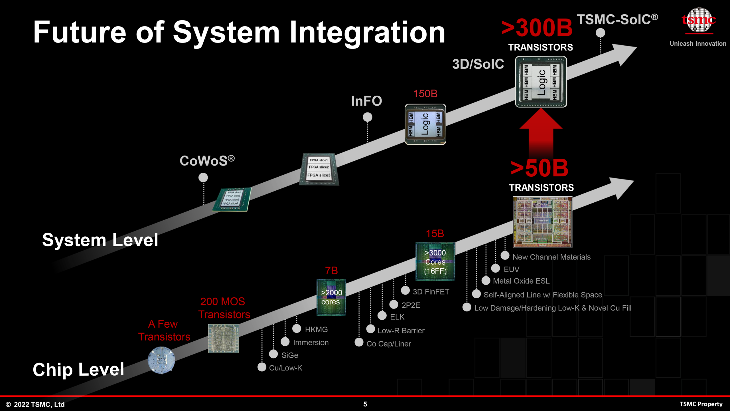
Enabling this kind of silicon and power growth has been modern technologies like TSMC'a CoWoS and InFO, which allow chipmakers to build integrated multi-chiplet system-in-packages (SiPs) with as much a double the amount of silicon otherwise allowed by TSMC's reticle limits. By 2024, advancements of TSMC's CoWoS packaging technology will enable building even larger multi-chiplet SiPs, with TSMC anticipating stitching together upwards of four reticle-sized chiplets, This will enable tremendous levels of complexity (over 300 billion transistor per SiP is a possibility that TSMC and its partners are looking at) and performance, but naturally at the cost of formidable power consumption and heat generation.
Already, flagship products like NVIDIA's H100 accelerator module require upwards of 700W of power for peak performance. So the prospect of multiple, GH100-sized chiplets on a single product is raising eyebrows – and power budgets. TSMC envisions that several years down the road there will be multi-chiplet SiPs with a power consumption of around 1000W or even higher, Creating a cooling challenge.
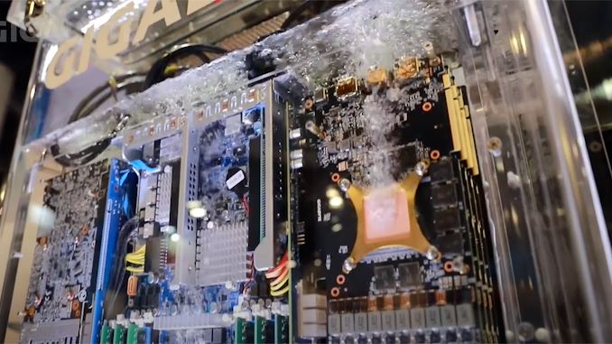
At 700W, H100 already requires liquid cooling; and the story is much the same for the chiplet based Ponte Vecchio from Intel, and AMD's Instinct MI250X. But even traditional liquid cooling has its limits. By the time chips reach a cumulative 1 kW, TSMC envisions that datacenters will need to use immersion liquid cooling systems for such extreme AI and HPC processors. Immersion liquid cooling, in turn, will require rearchitecting datacenters themselves, which will be a major change in design and a major challenge in continuity.
The short-tem challenges aside, once datacenters are setup for immersion liquid cooling, they will be ready for even hotter chips. Liquid immersion cooling has a lot of potential for handling large cooling loads, which is one reason why Intel is investing heavily in this technology in an attempt to make it more mainstream.
In addition to immersion liquid cooling, there is another technology that can be used to cool down ultra-hot chips — on-chip water cooling. Last year TSMC revealed that it had experimented with on-chip water cooling and said that even 2.6 kW SiPs could be cooled down using this technology. But of course, on-chip water cooling is an extremely expensive technology by itself, which will drive costs of those extreme AI and HPC solutions to unprecedented levels.
None the less, while the future isn't set in stone, seemingly it has been cast in silicon. TSMC's chipmaking clients have customers willing to pay a top dollar for those ultra-high-performance solutions (think operators of hyperscale cloud datacenters), even with the high costs and technical complexity that entails. Which to bring things back to where we started, is why TSMC has been developing CoWoS and InFO packaging processes on the first place – because there are customers ready and eager to break the reticle limit via chiplet technology. We're already seeing some of this today with products like Cerebras' massive Wafer Scale Engine processor, and via large chiplets, TSMC is preparing to make smaller (but still reticle-breaking) designs more accessible to their wider customer base.
Such extreme requirements for performance, packaging, and cooling not only push producers of semiconductors, servers, and cooling systems to their limits, but also require modifications of cloud datacenters. If indeed massive SiPs for AI and HPC workloads become widespread, cloud datacenters will be completely different in the coming years.


40 Comments
View All Comments
xol - Monday, June 27, 2022 - link
[carbon footprint] I'm just going to leave this here :https://www.dell.com/en-us/dt/corporate/social-imp... .. pick any
Generally the estimate is 85% impact during use, most of the remainder from manufacturing - this skews favor towards using the most efficient chips, and the lowest clocks..
There's also some alternate "life cycle assesments" (see LCA PowerEdge R6515 R7515 R6525 R7525) on the same page which give a slightly lower figure. It's clear from those alt links that 'silicon' is the vast majority of the impact from manufacture, and than includes both CPU, RAM and SSD -in fact SSD is typically >50%, RAM >25%, with Motherboard+CPU only 15%.
These figures kind of suprised me, but make sense having thought about it.
My conclusion would be that these figures make low clocks (ie low wattage CPU/thread) a no-brainer for carbon efficiency.
imo it's easier to de-carbonize server electrical supply than the whole supply/energy chain of chip manufacture - if that is an aim.
mode_13h - Monday, June 27, 2022 - link
> Generally the estimate is 85% impact during useThey don't account for maintenance of the hardware - just making, powering, and disposing of it.
> these figures make low clocks (ie low wattage CPU/thread) a no-brainer for carbon efficiency.
Again, you assume the workload scales to more cores, efficiently. Some algorithms don't.
The subject is HPC, not hyperscalers. If hyperscalers started using 1 kW processors, I'd be worried.
meacupla - Monday, June 27, 2022 - link
It's not just carbon footprint. When it comes to data centers, it's also water consumption.Google, for instance, doesn't want you, the public, to know how much fresh water they are consuming from the Colorado River, just to keep their data centers from overheating.
And the Colorado River is not exactly doing well when it comes to plentiful water.
mode_13h - Tuesday, June 28, 2022 - link
Hopefully, they just use that water in a closed loop, in which case there shouldn't really be any ongoing consumption.If they're dumping their waste heat as hot water downstream, someone should shut them down. Even worse would be simply evaporating the river water to cool their data center. Let's hope it's neither of those.
meacupla - Tuesday, June 28, 2022 - link
No, it's worse than that.Google is using evaporative cooling for their data centers sitting along the Colorado River. None of the water that gets used up goes back into the river.
All the water is wasted, and gets turned into very local high humidity.
mode_13h - Monday, July 4, 2022 - link
That's hard to believe.xol - Monday, June 27, 2022 - link
[more] there's limited info on carbon impact related to node size .. though this IMEC blog has some datahttps://www.imec-int.com/en/articles/environmental...
Though numbers get bigger as nodes get smaller up to 5nm they are not increasing faster than energy efficiency - which is good. At 3/2nm that may not be true but that info must be an estimate (?)
mode_13h - Monday, June 27, 2022 - link
I have a fantasy that CPUs will one day make the package into a vapor chamber, instead of using solder or thermal paste to conduct heat between the die and heat spreader. The benefit should be much more even heat distribution across the heat spreader, as well as better thermal conductivity between the dies and the heat spreader.Kevin G - Tuesday, June 28, 2022 - link
The challenge I see would be maintaining pressurization over time. Bonding the heat spreader to the substrate currently is not done to maintain a seal, much less at the pressures involved for a pure vapor chamber. Not a bad idea but it may require going back to ceramic packaging to pull it off due to how flexible substrates are currently.There is one added bonus to this though: you can have silicon stacks of different heights be cooled efficiently. Creating optimal heat spreaders requires some very precise machining which is rare. The more common solution being silicon shims to level off the stacks with material having the same thermal properties. Moving to a vapor chamber heat spreader removes those issues. I would be worried that the material in the vapor chamber is conductive and could get in between the silicon stacks.
This sounds like one of those wonderful engineering problems.
Doug_S - Monday, June 27, 2022 - link
There should be a decent energy efficiency gain using liquid cooling, as the power required for fans for servers, evaporators and high velocity movement of air inside the datacenter can be greatly reduced (depending on what remains to be cooled via forced air) with almost all power consumed for pumps and compressors only.