Intel: Sapphire Rapids With 64 GB of HBM2e, Ponte Vecchio with 408 MB L2 Cache
by Dr. Ian Cutress on November 15, 2021 9:00 AM EST
This week we have the annual Supercomputing event where all the major High Performance Computing players are putting their cards on the table when it comes to hardware, installations, and design wins. As part of the event Intel is having a presentation on its hardware offerings, which discloses additional details about the next generation hardware going into the Aurora Exascale supercomputer.
Aurora is a contract that Intel has had for some time – the scope was originally to have a 10nm Xeon Phi based system, for which the idea was mothballed when Xeon Phi was scrapped, and has been an ever changing landscape due to Intel’s hardware offerings. It was finalized a couple of years ago that the system would now be using Intel’s Sapphire Rapids processors (the ones that come with High Bandwidth Memory) combined with new Ponte Vecchio Xe-HPC based GPU accelerators and boosted from several hundred PetaFLOPs to an ExaFLOP of compute. Most recently, Intel CEO Pat Gelsinger has disclosed that the Ponte Vecchio accelerator is achieving double the performance, above the expectations of the original disclosures, and that Aurora will be a 2+EF Supercomputer when built. Intel is expecting to deliver the first batch of hardware to the Argonne National Laboratory by the end of the year, but this will come with $300m write-off on Intel’s Q4 financials. Intel is expecting to deliver the rest of the machine through 2022 as well as ramp up the production of the hardware for mainstream use through Q1 for wider spread launch in the first half of the year.
Today we have additional details about the hardware.
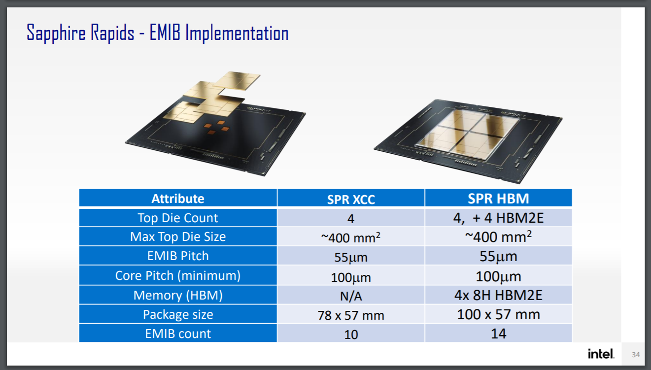
On the processor side, we know that each unit of Aurora will feature two of Intel’s newest Sapphire Rapids CPUs (SPR), featuring four compute tiles, DDR5, PCIe 5.0, CXL 1.1 (not CXL.mem), and will be liberally using EMIB connectivity between the tiles. Aurora will also be using SPR with built-in High Bandwidth Memory (SPR+HBM), and the main disclosure is that SPR+HBM will offer up to 64 GB of HBM2e using 8-Hi stacks.
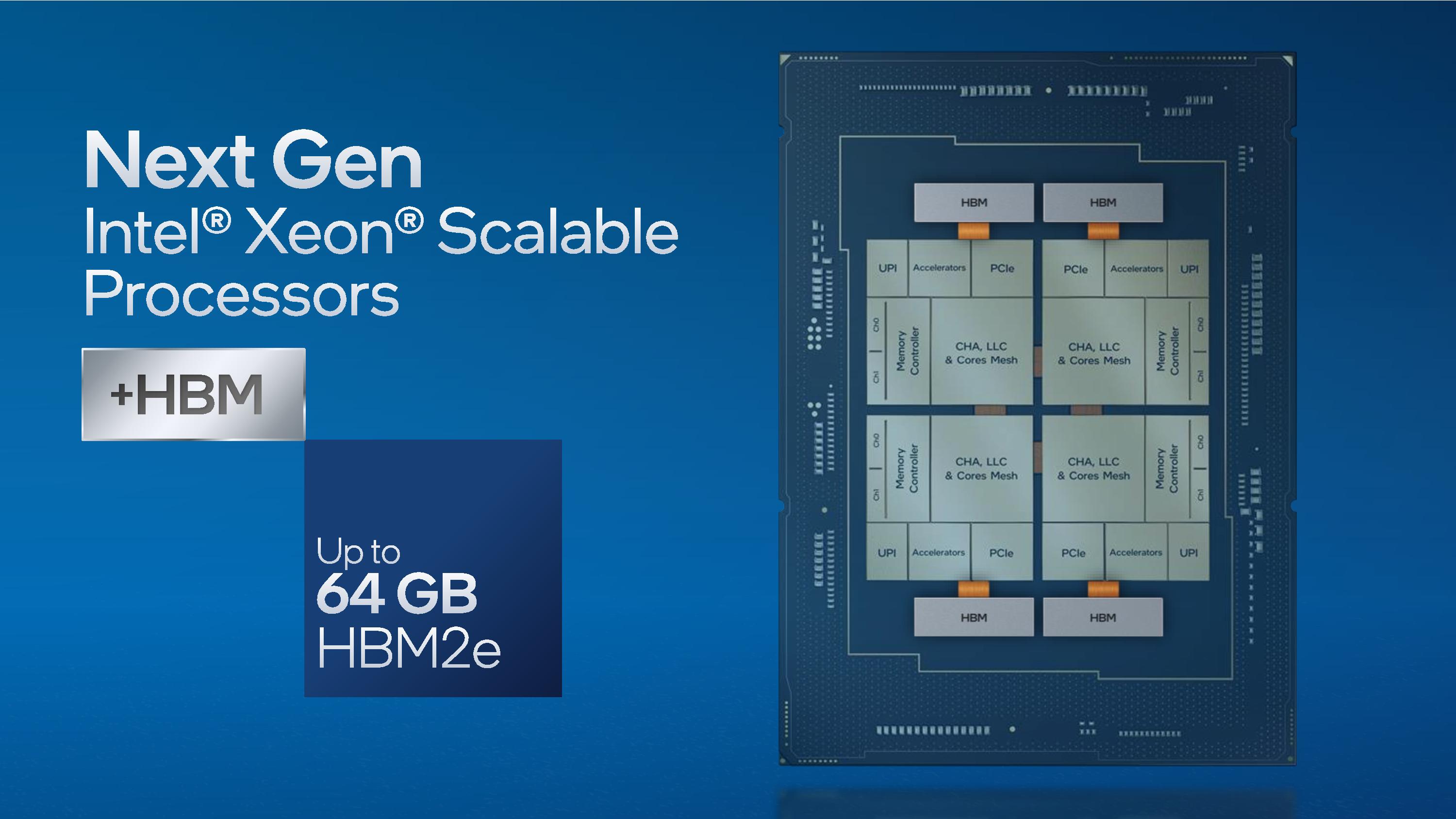
Based on the representations, Intel intends to use four stacks of 16 GB HBM2e for a total of 64 GB. Intel has a relationship with Micron, and the Micron HBM2e physical dimensions are in line with the representations given in Intel’s materials (compared to say, Samsung or SKHynix). Micron currently offers two versions of 16 GB HBM2E with ECC hardware: one at 2.8 Gbps per pin (358 GB/s per stack) and one at 3.2 Gbps per pin (410 GB/s per stack). Overall we’re looking at a peak bandwidth then between 1.432 TB/s to 1.640 TB/s depending on which version Intel is using. Versions with HBM will use an additional four tiles, to connect each HBM stack to one of SPR’s chiplets.
Based on this diagram from Intel, despite Intel stating that SPR+HBM will share a socket with traditional SPR, it’s clear that there will be versions that are not compatible. This may be an instance where the Aurora versions of SPR+HBM are tuned specifically for that machine.
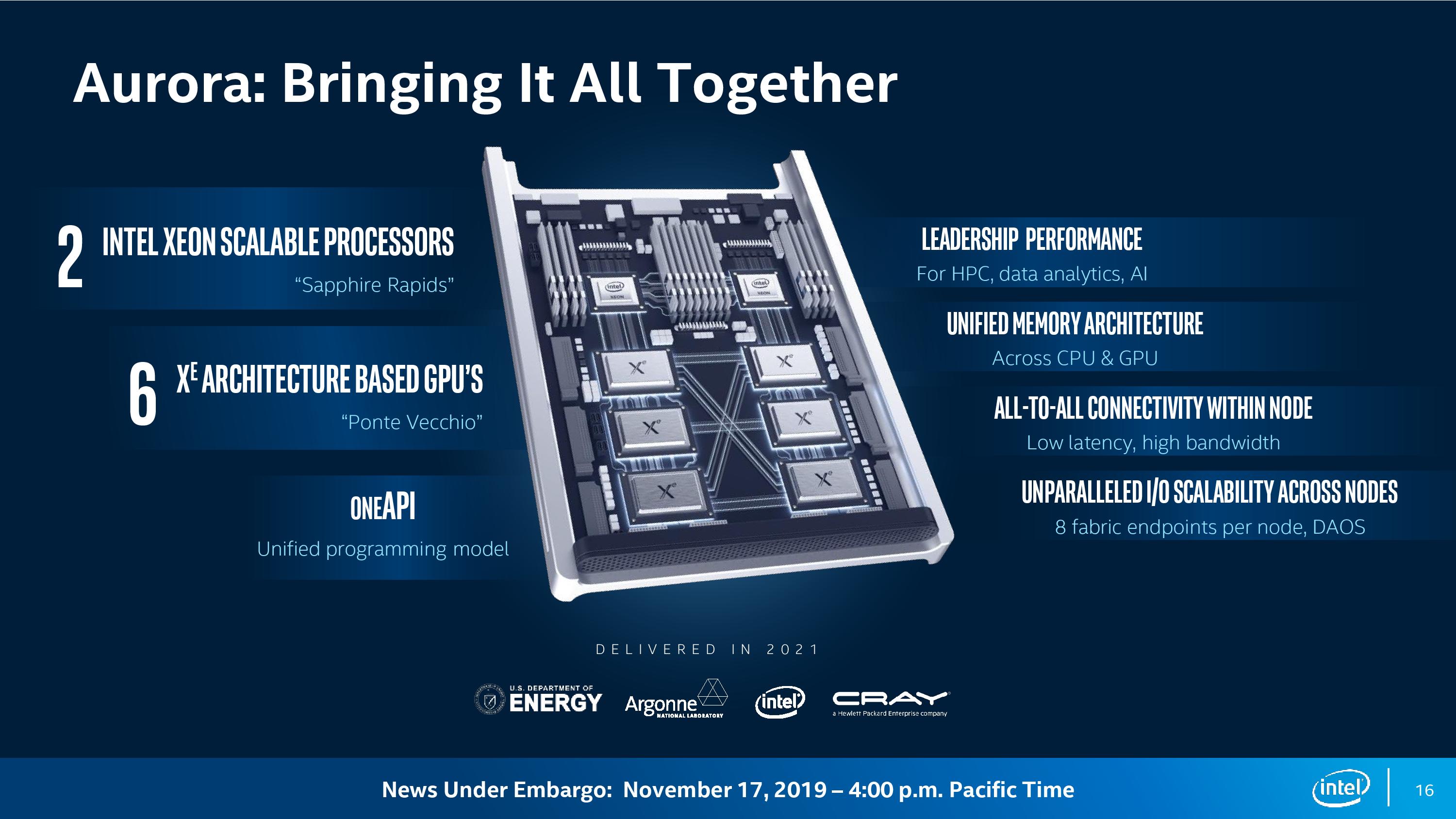
On the Ponte Vecchio (PVC) side of the equation, Intel has already disclosed that a single server inside Aurora will have six PVC accelerators per two SPR processors. Each of the accelerators will be connected in an all-to-all topology to each other using the new Xe-Link protocol built into each PVC – Xe-Link supports 8 in fully connected mode, so Aurora only needing six of those saves more power for the hardware. It’s not been disclosed how they are connected to the SPR processors – Intel has stated that there will be a unified memory architecture between CPU and GPU.
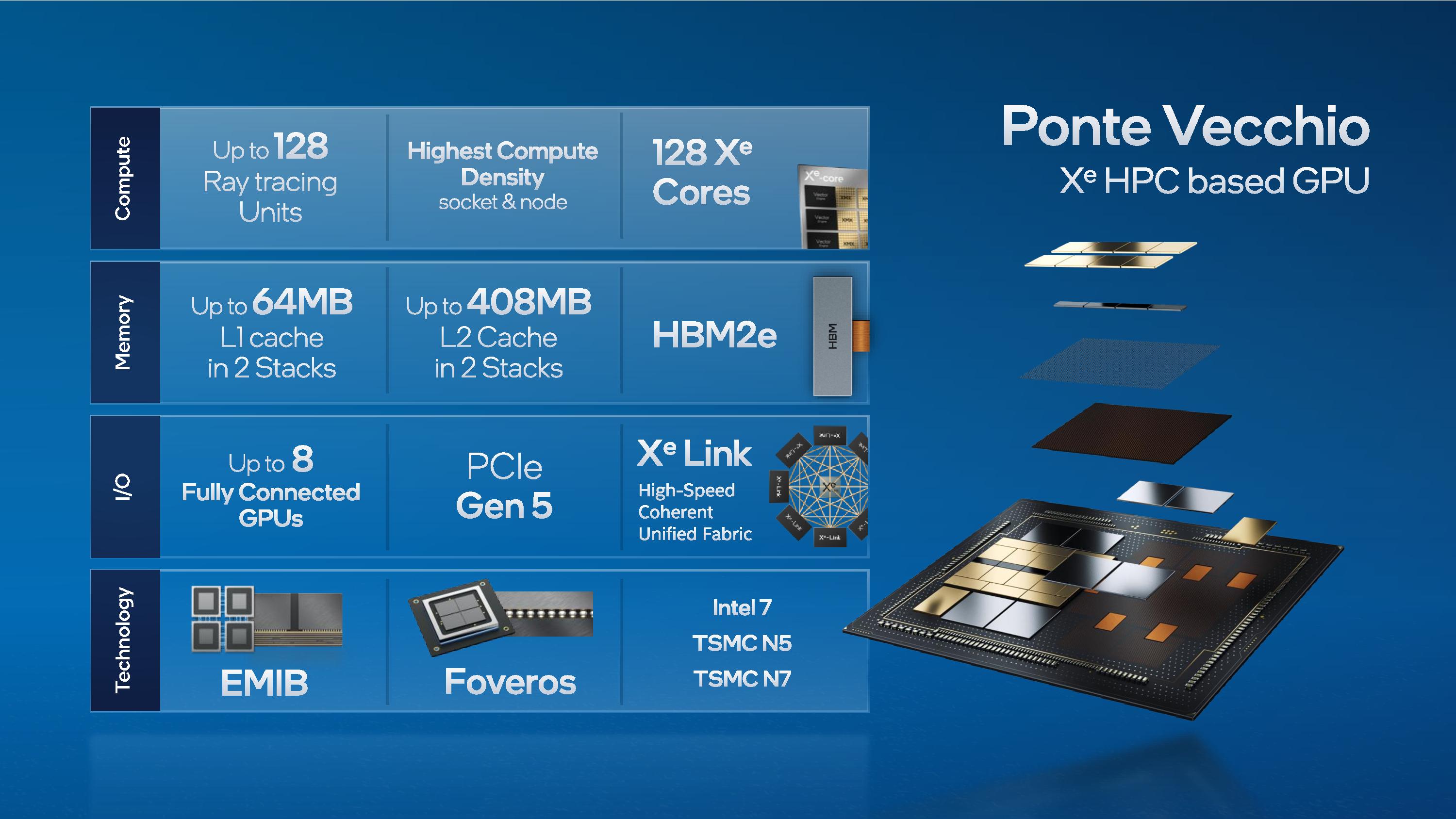
The insight added today by Intel is that each Ponte Vecchio dual-stack implementation (the diagram Intel has shown repeatedly is two stacks side by side) will feature a total of 64 MB of L1 cache and 408 MB of L2 cache, backed by HBM2e.
408 MB of L2 cache across two stacks means 204 MB per stack. If we compare that to other hardware:
- NVIDIA A100 has 40 MB of L2 cache
- AMD’s Navi 21 has 128 MB of Infinity Cache (an effective L3)
- AMD’s CNDA2 MI250X in Frontier has 8 MB of L2 per ‘stack’, or 16 MB total
Whichever way you slice it, Intel is betting hard on having the right hierarchy of cache for PVC. Diagrams of PVC also show 4 HBM2e chips per half, which suggests that each PVC dual-stack design might have 128 GB of HBM2e. It is likely that none of them are ‘spare’ for yield purposes, as a chiplet based design allows Intel to build PVC using known good die from the beginning.
On top of this, we also get an official number as to the scale of how many Ponte Vecchio GPUs and Sapphire Rapids (+HBM) processors we need for Aurora. Back in November 2019, when Aurora was only listed as a 1EF supercomputer, I crunched some rough numbers based on Intel saying Aurora was 200 racks and making educated guesses on the layout – I got to 5000 CPUs and 15000 GPUs, with each PVC needing around 66.6TF of performance. At the time, Intel was already showing off 40 TF of performance per card on early silicon. Intel’s official numbers for the Aurora 2EF machine are:
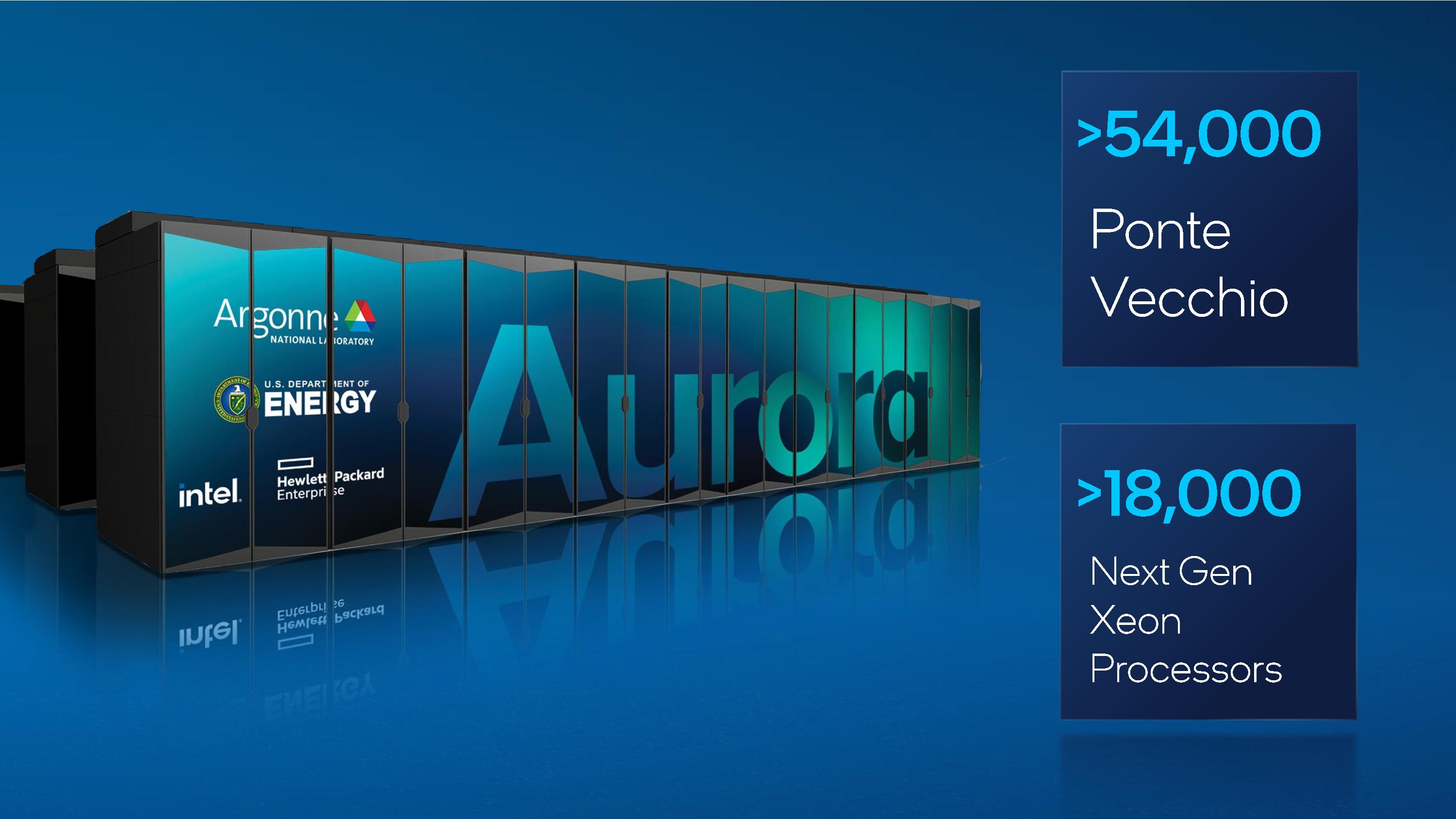
18000+ CPUs and 54000+ GPUs is a lot of hardware. But dividing 2 Exaflops by 54000 PVC accelerators comes to only 37 TeraFlops per PVC as an upper bound, and that number is assuming zero performance is coming from the CPUs.
To add into the mix: Intel CEO Pat Gelsinger only a couple of weeks ago said that PVC was coming in at double the performance originally expected, allowing Aurora to be a 2EF machine. Does that mean the original performance target for PVC was ~20 TF of FP64? Apropos of nothing, AMD’s recent MI250X announcement last week showcased a dual-GPU chip with 47.9 TF of FP64 vector performance, moving to 95.7 TF in FP64 matrix performance. The end result here might be that AMD’s MI250X is actually higher raw performance than PVC, however AMD requires 560 W for that card, whereas Intel’s power numbers have not been disclosed. We could do some napkin math here as well.
- Frontier uses 560 W MI250X cards, and is rated for 1.5 ExaFlops of FP64 Vector at 30 MW of power. This means Frontier needs 31300 cards (1.5 EF / 49.7 TF) to meet performance targets, and for each 560 W MI250X card, Frontier has allocated 958 Watts of power (30 MW / 31300 cards). This is a 71% overhead for each card (which means cooling, storage systems, other compute/management etc).
- Aurora uses PVC at an unknown power, is rated for 2 ExaFlops of FP64 Vector at 60 MW of power. We know that PVC has 54000+ cards to meet performance targets, which means that the system has allocated 1053 W (that’s 60 MW / 54000) per card to include the PVC accelerator and other overheads required. If we were to assume (a big assumption I know) that Frontier and Aurora have similar overheads, then we’re looking at 615 W per PVC.
- This would end up with PVC at 615 W for 37 TF, against MI250X at 560 W for 47.9 TF.
- This raw discussion fails to discuss specific features each card has for its use case.
| Compute GPU Accelerator Comparison Confirmed Numbers |
|||
| AnandTech | Intel | AMD | NVIDIA |
| Product | Ponte Vecchio | MI250X | A100 80GB |
| Architecture | Xe-HPC | CDNA2 | Ampere |
| Transistors | 100 B | 58.2 B | 54.2 B |
| Tiles (inc HBM) | 47 | 10 | 6 + 1 spare |
| Compute Units | 128 | 2 x 110 | 108 |
| Matrix Cores | 128 | 2 x 440 | 432 |
| INT8 Tensor | ? | 383 TOPs | 624 TOPs |
| FP16 Matrix | ? | 383 TOPs | 312 TOPs |
| FP64 Vector | ? | 47.9 TFLOPS | 9.5 TFLOPS |
| FP64 Matrix | ? | 95.7 TFLOPs | 19.5 TFLOPS |
| L2 / L3 | 2 x 204 MB | 2 x 8 MB | 40 MB |
| VRAM Capacity | 128 GB (?) | 128 GB | 80 GB |
| VRAM Type | 8 x HBM2e | 8 x HBM2e | 5 x HBM2e |
| VRAM Width | ? | 8192-bit | 5120-bit |
| VRAM Bandwidth | ? | 3.2 TB/s | 2.0 TB/s |
| Chip-to-Chip Total BW | 8 | 8 x 100 GB/s | 12 x 50 GB/s |
| CPU Coherency | Yes | With IF | With NVLink 3 |
| Manufacturing | Intel 7 TSMC N7 TSMC N5 |
TSMC N6 | TSMC N7 |
| Form Factors | OAM | OAM (560 W) | SXM4 (400W*) PCIe (300W) |
| Release Date | 2022 | 11/2021 | 11/2020 |
| *Some Custom deployments go up to 600W | |||
Intel also disclosed that it will be partnering with SiPearl to deploy PVC hardware in the European HPC efforts. SiPearl is currently building an Arm-based CPU called Rhea built on TSMC N7.
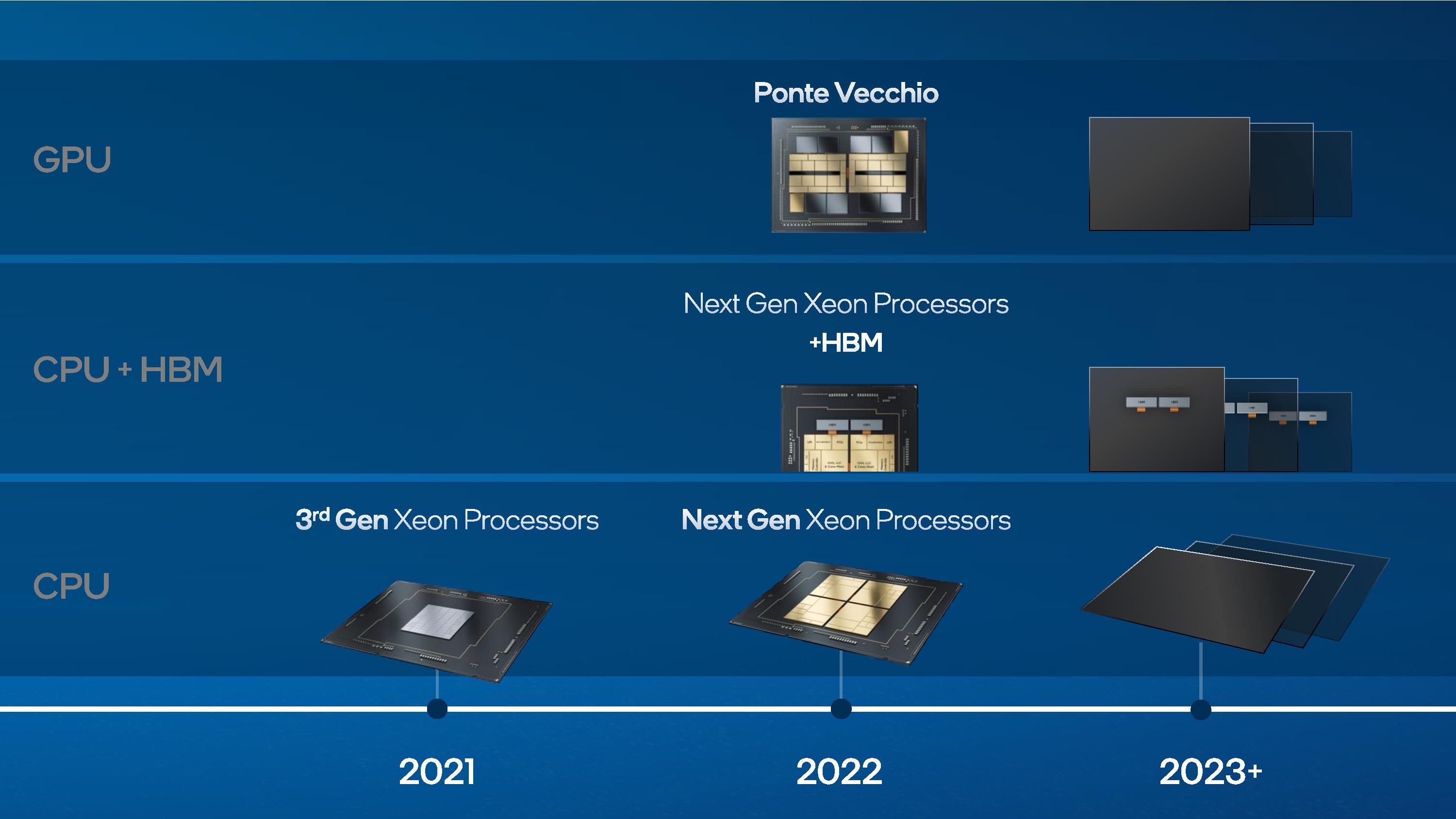
Moving forward, Intel also released a mini-roadmap. Nothing too surprising here - Intel has plans for designs beyond Ponte Vecchio, and that future Xeon Scalable processors will also have options enabled with HBM.
Related Reading
- Intel's Aurora Supercomputer Now Expected to Exceed 2 ExaFLOPS Performance
- Intel Teases Ponte Vecchio Xe-HPC Power On, Posts Photo of Server Chip
- Analyzing Intel’s Discrete Xe-HPC Graphics Disclosure: Ponte Vecchio, Rambo Cache, and Gelato
- Intel’s 2021 Exascale Vision in Aurora: Two Sapphire Rapids CPUs with Six Ponte Vecchio GPUs
- Intel’s Xe for HPC: Ponte Vecchio with Chiplets, EMIB, and Foveros on 7nm, Coming 2021
- Bringing Geek Back: Q&A with Intel CEO Pat Gelsinger
- Intel Architecture Day 2021: A Sneak Peek At The Xe-HPG GPU Architecture
- Intel to Launch Next-Gen Sapphire Rapids Xeon with High Bandwidth Memory
- Intel’s Xeon & Xe Compute Accelerators to Power Aurora Exascale Supercomputer
- SiPearl Lets Rhea Design Leak: 72x Zeus Cores, 4x HBM2E, 4-6 DDR5
- AMD Announces Instinct MI200 Accelerator Family: Taking Servers to Exascale and Beyond


69 Comments
View All Comments
abufrejoval - Monday, November 15, 2021 - link
I was going to ask: "But can it run FarCry?"...But I guess the only question to ask is how many instances of FarCry can an Exaflop deliver--just to put things into perspective.
These are awsome chunks of silicon!
I just wonder what SiPearl is now doing with Intel. The original design was something like Fujitsu's ARM CPU and then a completely new RISC-V based vector/matrix accelerator unit.
I guess that latter part has now been scrapped for a less ambitious PVC based design? I can't quite see how that fulfills the original "independence" criteria, though.
JayNor - Monday, November 15, 2021 - link
I'm guessing Raja's recent visit to BSC wasn't just a pleasure trip.TanjB - Saturday, November 27, 2021 - link
It could run you, and your opponents, running FarCry. To exit, you will need to locate a red pill.JayNor - Monday, November 15, 2021 - link
so is this 408GB the Rambo Cache?I presume it is the grid of L2 cache shown in the recent patent app ... covering the whole base tile.
The patent app says it is re-configurable at boot to be shared or local. Any details?
The Hardcard - Monday, November 15, 2021 - link
Is that L2 amount for the M250X from an official source? 16 MB is surprisingly low.dotted - Tuesday, November 16, 2021 - link
AMD's own white paper on CDNA2 lists 8MB of L2 per graphics compute die.mode_13h - Thursday, November 18, 2021 - link
GPUs typically have a very small amount of L2. I think it's mainly used to aggregate memory accesses. The cost/benefit analysis probably doesn't support adding much L2, given how high the turnover rate would be. Also, if data is typically streamed into the GPU each time it's used, then a bigger cache wouldn't necessarily provide the same degree of benefit as in a CPU.I wonder if Intel's seeming reliance on L2 is to compensate for their traditionally smaller number of SMT threads. Latency-hiding is one of the main roles of SMT, especially in GPUs. If it's falling short, then it makes sense that you'd resort to other tricks, like massive caches.
Oxford Guy - Monday, November 15, 2021 - link
Unless the ‘specific features each card has for its use case’ is the trump card for Intel here, it looks like the company is throwing a disproportionately huge number of transistors at FP (100B vs. 58.2) and getting worse performance-per-watt than AMD.AMD’s design greatly outperforms Nvidia’s for FP-64 but lags in Tensor. So, I assume there is something other than FP-64 the design is dedicating so many transistors to.
Am I missing something?
LightningNZ - Monday, November 15, 2021 - link
I don't think we have a clear idea of how they perform in practice yet. There are some vendor released benchmarks for AMD, Intel's performance is still a mystery, peak FLOPs be damned. I'm sure the actual performance of each is highly dependent on the workload, though you're right to question why Intel is putting so much cache on these chips when it appears to hurt their power consumption so badly. What workloads have this much locality and reuse? MostHPC codes that I'm familiar with (not many) use fairly small kernels and then pass their results on. Perhaps there is a new HPC paradigm that Argonne want to address?
Spunjji - Wednesday, November 17, 2021 - link
"you're right to question why Intel is putting so much cache on these chips when it appears to hurt their power consumption so badly"It's possible that the cache is keeping things in check where without it they'd be even worse. Xe-LP wasn't that great for power efficiency vs. Vega and CDNA 2 is a couple of generations improved from that, with a specific focus on FP64. AMD are also a bit further ahead than Intel with integrating multiple dies.