Intel Xeon Sapphire Rapids: How To Go Monolithic with Tiles
by Dr. Ian Cutress on August 31, 2021 10:00 AM EST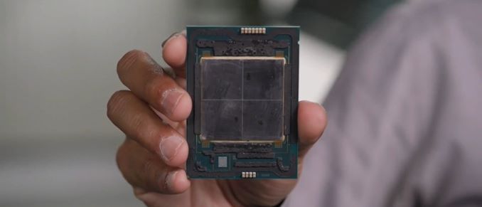
One of the critical deficits Intel has to its competition in its server platform is core count – other companies are enabling more cores by one of two routes: smaller cores, or individual chiplets connected together. At its Architecture Day 2021, Intel has disclosed features about its next-gen Xeon Scalable platform, one of which is the move to a tiled architecture. Intel is set to combine four tiles/chiplets through its fast embedded bridges, leading to better CPU scalability at higher core counts. As part of the disclosure, Intel also expanded on its new Advanced Matrix Extension (AMX) technology, CXL 1.1 support, DDR5, PCIe 5.0, and an Accelerator Interfacing Architecture that may lead to custom Xeon CPUs in the future.
What is Sapphire Rapids?
Built on an Intel 7 process, Sapphire Rapids (SPR) will be Intel’s next-generation Xeon Scalable server processor for its Eagle Stream platform. Using its latest Golden Cove processor cores which we detailed last week, Sapphire Rapids will bring together a number of key technologies for Intel: Acceleration Engines, native half-precision FP16 support, DDR5, 300-Series Optane DC Persistent Memory, PCIe 5.0, CXL 1.1, a wider and faster UPI, its newest bridging technology (EMIB), new QoS and telemetry, HBM, and workload specialized acceleration.
Set to launch in 2022, Sapphire Rapids will be Intel’s first modern CPU product to take advantage of a multi-die architecture that aims to minimize latency and maximize bandwidth due to its Embedded Multi-Die Interconnect Bridge technology. This allows for more high-performance cores (Intel hasn’t said how many just quite yet), with the focus on ‘metrics that matter for its customer base, such as node performance and data center performance’. Intel is calling SPR the ‘Biggest Leap in DC Capabilities in a Decade’.
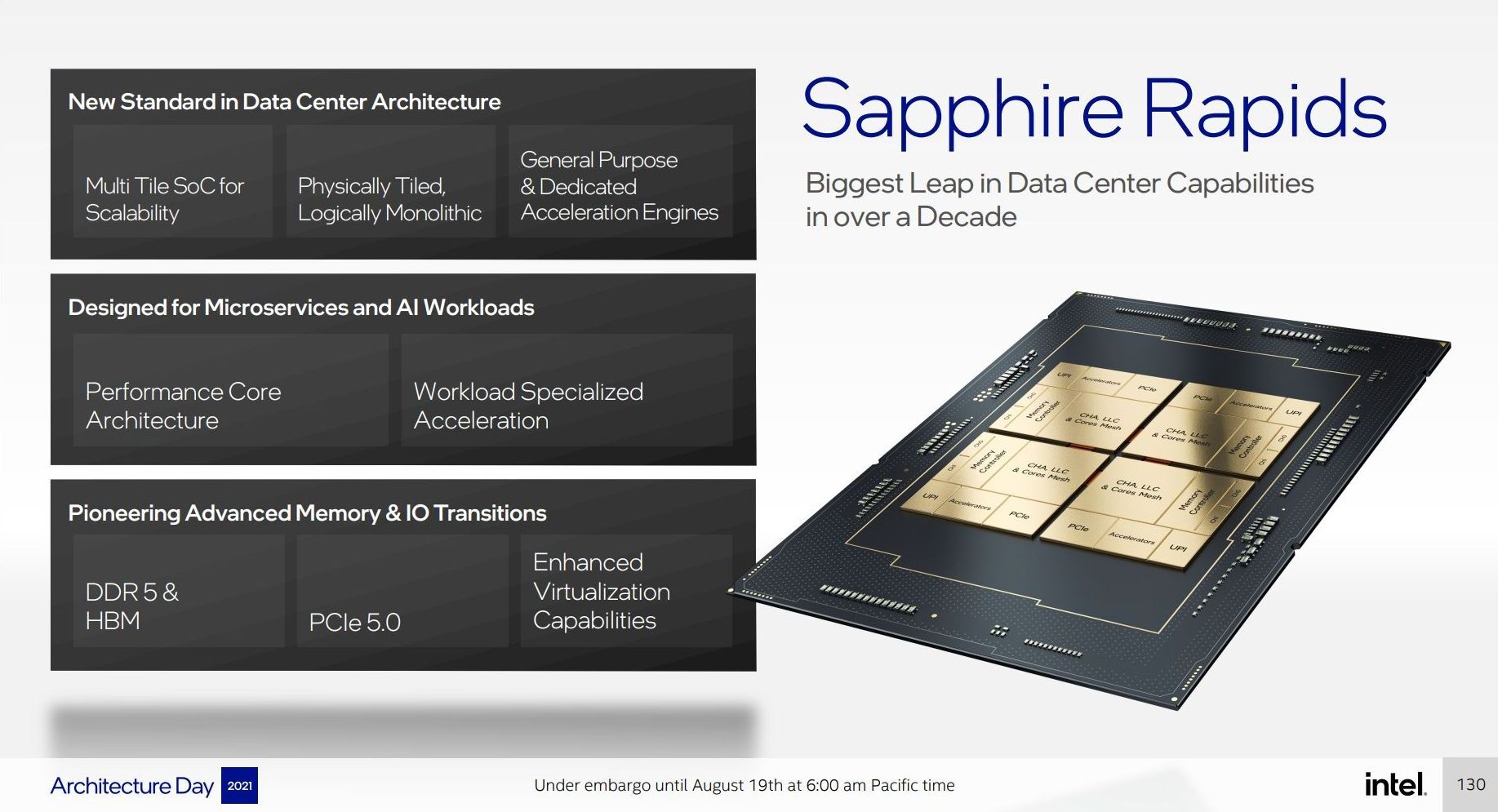
The headline benefits are easy to rattle off. PCIe 5.0 is an upgrade over the previous generation Ice Lake PCIe 4.0, and we move from six 64-bit memory controllers of DDR4 to eight 64-bit memory controllers of DDR5. But the bigger improvements are in the cores, the accelerators, and the packaging.
Golden Cove: A High-Performance Core with AMX and AIA
By using the same core design on its enterprise platform Sapphire Rapids and consumer platform Alder Lake, there are some of the same synergies we saw back in the early 2000s when Intel did the same thing. We covered Golden Cove in detail in our Alder Lake architecture deep dive, however here’s a quick recap:
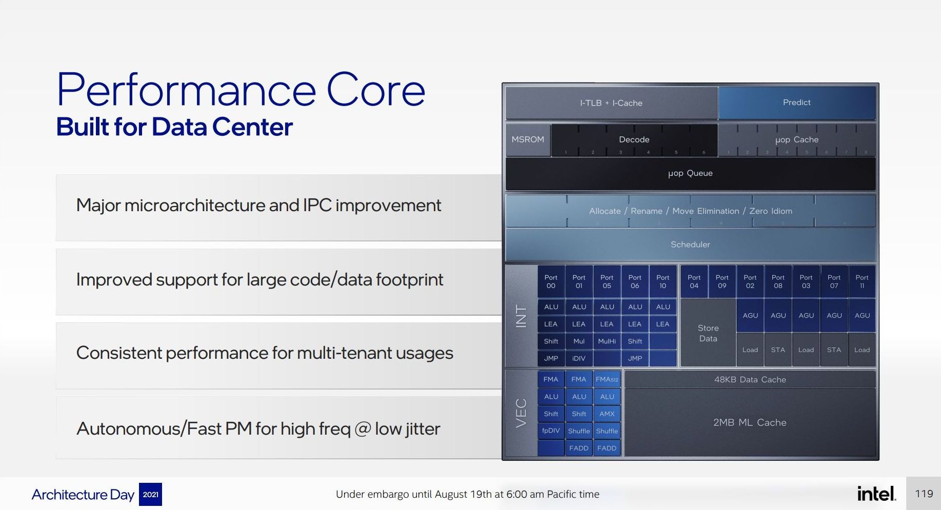
The new core, according to Intel, will over a +19% IPC gain in single-thread workloads compared to Cypress Cove, which was Intel’s backport of Ice Lake. This comes down to some big core changes, including:
- 16B → 32B length decode
- 4-wide → 6-wide decode
- 5K → 12K branch targets
- 2.25K → 4K μop cache
- 5 → 6 wide allocation
- 10 → 12 execution ports
- 352 → 512-entry reorder buffer
The goal of any core is to process more things faster, and the newest generation tries to do it better than before. A lot of Intel’s changes make sense, and those wanting the deeper details are encouraged to read our deep dive.
There are some major differences between the consumer version of this core in Alder Lake and the server version in Sapphire Rapids. The most obvious one is that the consumer version does not have AVX-512, whereas SPR will have it enabled. SPR also has a 2 MB private L2 cache per core, whereas the consumer model has 1.25 MB. Beyond this, we’re talking about Advanced Matrix Extensions (AMX) and a new Accelerator Interface Architecture (AIA).
So far in Intel’s CPU cores we have scalar operation (normal) and vector operation (AVX, AVX2, AVX-512). The next stage up from that is a dedicated matrix solver, or something akin to a tensor core in a GPU. This is what AMX does, by adding a new expandable register file with dedicated AMX instructions in the form of TMUL instructions.
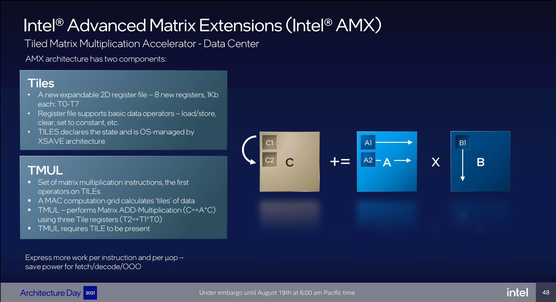
AMX uses eight 1024-bit registers for basic data operators, and through memory references, the TMUL instructions will operate on tiles of data using those tile registers. The TMUL is supported through a dedicated Engine Coprocessor built into the core (of which each core has one), and the basis behind AMX is that TMUL is only one such co-processor. Intel has designed AMX to be wider-ranging than simply this – in the event that Intel goes deeper with its silicon multi-die strategy, at some point we could see custom accelerators being enabled through AMX.
Intel confirmed that we shouldn’t see any frequency dips worse than AVX – there are new fine-grained power controllers per core for when vector and matrix instructions are invoked.

This feeds quite nicely into discussing AIA, the new accelerator interface. Typically when using add-in accelerator cards, commands must navigate between kernel and user space, set up memory, and direct any virtualization between multiple hosts. The way Intel is describing its new Acceleration Engine interface is akin to talking to a PCIe device as if it were simply an accelerator on board to the CPU, even though it’s attached through PCIe.

Initially, Intel will have two capable AIA bits of hardware.
Intel Quick Assist Technology (QAT) is one we’ve seen before, as it showcased inside special variants of Skylake Xeon’s chipset (that required a PCIe 3.0 x16 link) as well as an add-in PCIe card – this version will support up to 400 Gb/s symmetric cryptography, or up to 160 Gb/s compression plus 160 Gb/s decompression simultaneously, double the previous version.
The other is Intel’s Data Streaming Accelerator (DSA). Intel has had documentation about DSA on the web since 2019, stating that it is a high-performance data copy and transformation accelerator for streaming data from storage and memory or to other parts of the system through a DMA remapping hardware unit/IOMMU. DSA has been a request from specific hyperscaler customers, who are looking to deploy it within their own internal cloud infrastructure, and Intel is keen to point out that some customers will use DSA, some will use Intel’s new Infrastructure Processing Unit, while some will use both, depending on what level of integration or abstraction they are interested in. Intel told us that DSA is an upgrade over the Crystal Beach DMA engine which was present on the Purley (SKL+CLX) platforms.
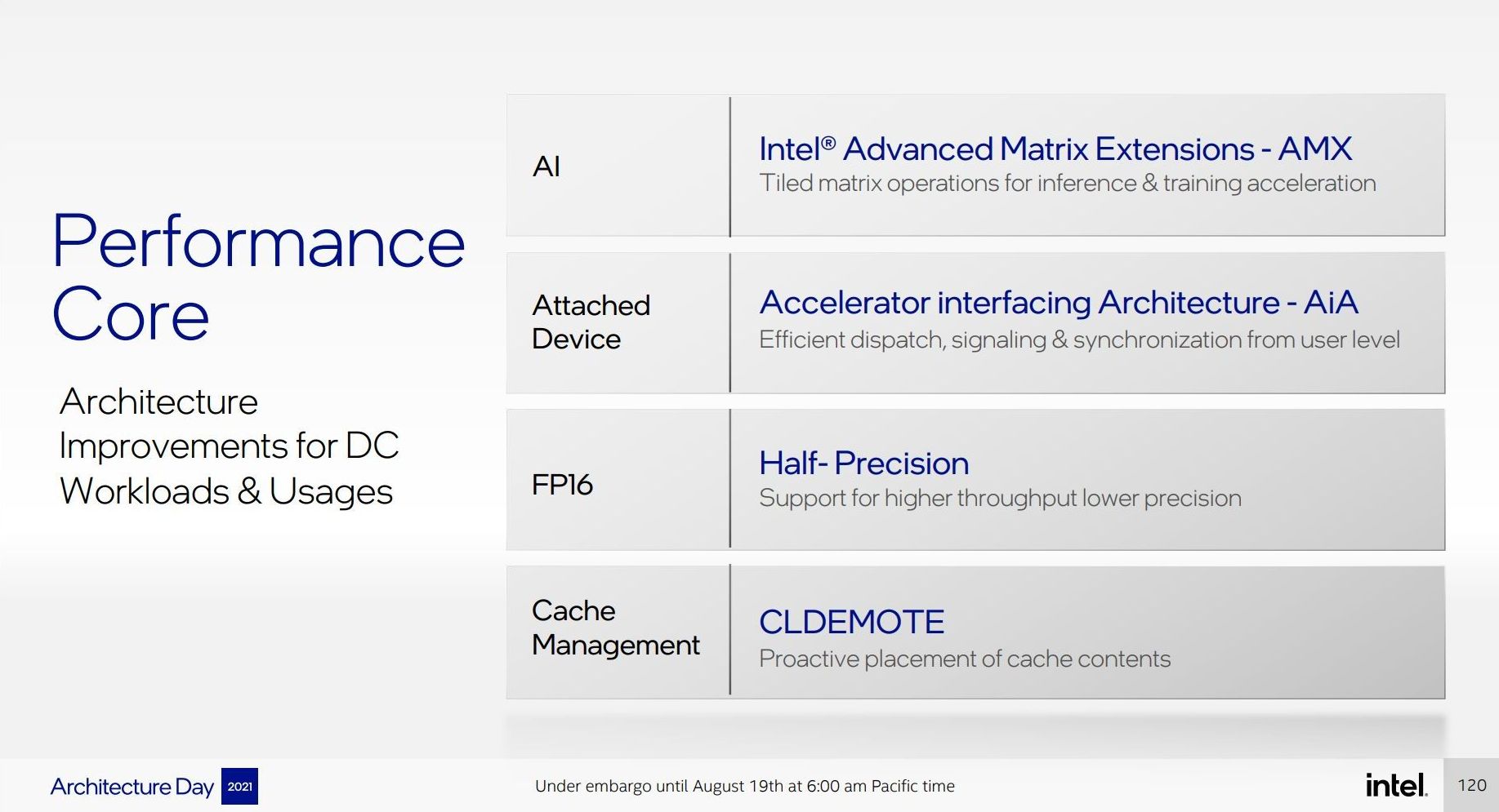
On top of all this, Sapphire Rapids also supports AVX512_FP16 instructions for half-precision, mostly for AI workloads as part of its DLBoost strategy (Intel was quite quiet on DLBoost during the event). These FP16 commands can also be used as part of AMX, alongside INT8 and BF16 support. Intel now also supports CLDEMOTE for cache-line management.
A Side Word about CXL
Throughout the presentations of Sapphire Rapids, Intel has been keen to highlight it will support CXL 1.1 at launch. CXL is a connectivity standard designed to handle much more than what PCIe does – aside from simply acting as a data transfer from host to device, CXL has three branches to support, known as IO, Cache, and Memory. As defined in the CXL 1.0 and 1.1 standards, these three form the basis of a new way to connect a host with a device.
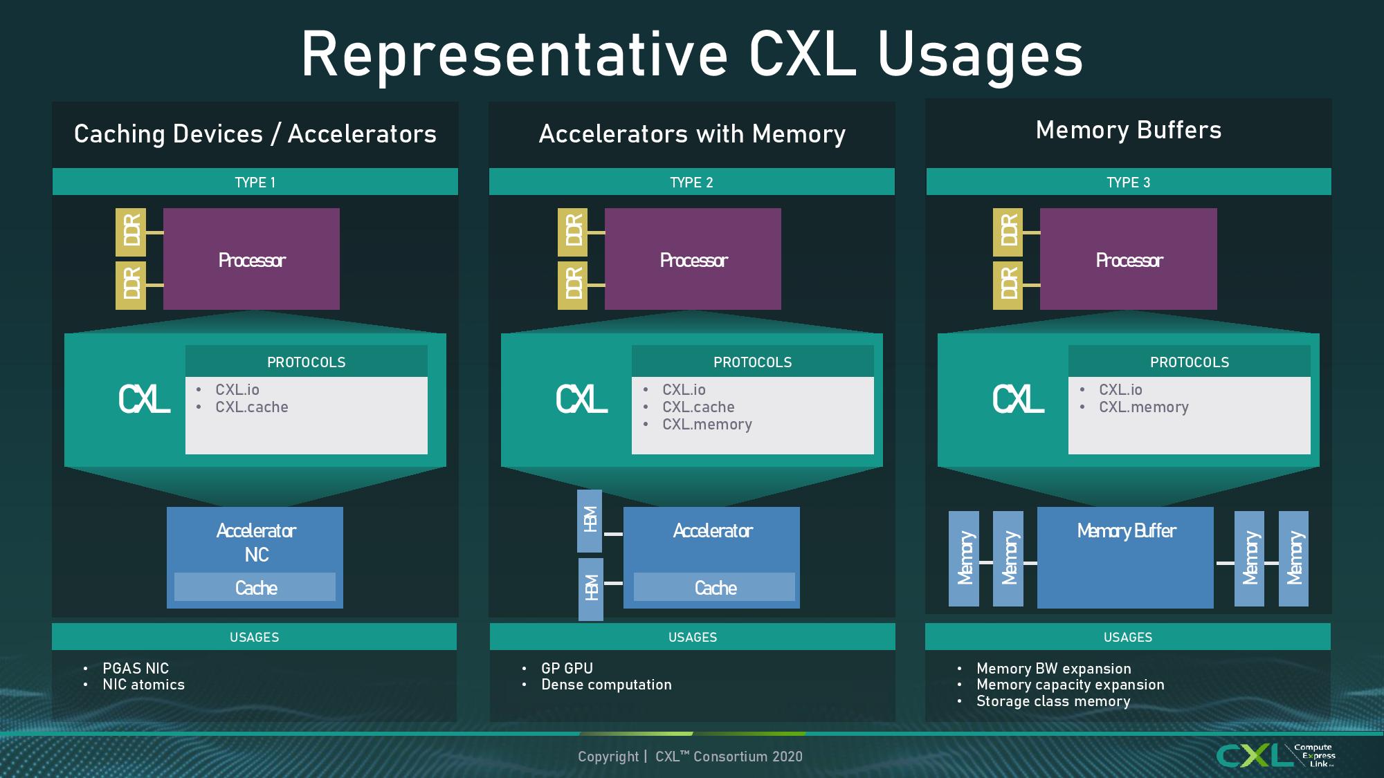
Naturally it was our expectation that all CXL 1.1 devices would support all three of these standards. It wasn’t until Hot Chips, several days later, that we learned Sapphire Rapids is only supporting part of the CXL standard, specifically CXL.io and CXL.cache, but CXL.memory would not be part of SPR. We're not sure to what extent this means SPR isn't CXL 1.1 compliant, or what it means for CXL 1.1 devices - without CXL.mem, as per the diagram above, all Intel loses is Type-2 support. Perhaps this is more of an indication that the market around CXL is better served by CXL 2.0, which will no doubt come in a later product.
In the next page, we look at Intel's new tiled architecture for Sapphire Rapids.


94 Comments
View All Comments
Wrs - Tuesday, August 31, 2021 - link
The "glue" is everything, though. Whole article is really about that. Gotta characterize and benchmark it. At least on paper it looks very good, better than AMD'sdullard - Tuesday, August 31, 2021 - link
yannigr2 was referring to just about everyone (even our very own Anand) calling the Pentium D two cores glued together. https://www.anandtech.com/show/1665/2 It is an old joke.heickelrrx - Friday, September 3, 2021 - link
it's not a gluebut ducktape
Yojimbo - Tuesday, August 31, 2021 - link
"The new core, according to Intel, will over a +19% IPC gain in single-thread workloads compared to Cypress Cove, which was Intel’s backport of Ice Lake."I think Cypress Cove is a backport of Willow Cove. Ice Lake uses Sunny Cove. There isn't much IPC improvement from Sunny Cove to Willow Cove, if I recall, so 19% IPC over Ice Lake might still be accurate even if the information given is technically wrong.
yeeeeman - Tuesday, August 31, 2021 - link
Actually there isn't much IPC improvement even from sunny cove to willow cove.Yojimbo - Tuesday, August 31, 2021 - link
You repeated something I already had written.shabby - Tuesday, August 31, 2021 - link
Intels idea of ipc improvement come from the higher mhz the chip runs at, they're skewing what ipc means.Yojimbo - Tuesday, August 31, 2021 - link
No it doesn't.Foeketijn - Wednesday, September 1, 2021 - link
yes it does. IPC is performance per hz. Double the speed, double the performance means same IPC.Yojimbo - Wednesday, September 1, 2021 - link
The "it" in my sentence referred to Intel. Intel doesn't include clock speed increase in its measure of IPC increase. Intel compares "iso-freq" (same frequency) as per this graphic for Sunny Cove over Skylake https://images.anandtech.com/doci/14514/Blueprint%......or this one for Golden Cove over Cypress Cove.