The AMD Ryzen 7 5700G, Ryzen 5 5600G, and Ryzen 3 5300G Review
by Dr. Ian Cutress on August 4, 2021 1:45 PM ESTPower Consumption
The nature of reporting processor power consumption has become, in part, a dystopian nightmare. Historically the peak power consumption of a processor, as purchased, is given by its Thermal Design Power (TDP, or PL1). For many markets, such as embedded processors, that value of TDP still signifies the peak power consumption. For the processors we test at AnandTech, either desktop, notebook, or enterprise, this is not always the case.
Modern high-performance processors implement a feature called Turbo. This allows, usually for a limited time, a processor to go beyond its rated frequency. Exactly how far the processor goes depends on a few factors, such as the Turbo Power Limit (PL2), whether the peak frequency is hardcoded, the thermals, and the power delivery. Turbo can sometimes be very aggressive, allowing power values 2.5x above the rated TDP.
AMD and Intel have different definitions for TDP, but are broadly speaking applied the same. The difference comes to turbo modes, turbo limits, turbo budgets, and how the processors manage that power balance. These topics are 10000-12000 word articles in their own right, and we’ve got a few articles worth reading on the topic.
- Why Intel Processors Draw More Power Than Expected: TDP and Turbo Explained
- Talking TDP, Turbo and Overclocking: An Interview with Intel Fellow Guy Therien
- Reaching for Turbo: Aligning Perception with AMD’s Frequency Metrics
- Intel’s TDP Shenanigans Hurts Everyone
In simple terms, processor manufacturers only ever guarantee two values that are tied together - when all cores are running at base frequency, the processor should be running at or below the TDP rating. All turbo modes and power modes above that are not covered by warranty. Intel kind of screwed this up with the Tiger Lake launch in September 2020, by refusing to define a TDP rating for its new processors, instead of going for a range. Obfuscation like this is a frustrating endeavor for press and end-users alike.
However, for our tests in this review, we measure the power consumption of the processor in a variety of different scenarios. These include workflows, real-world image-model construction, and others as appropriate. These tests are done as comparative models. We also note the peak power recorded in any of our tests.
First up is our image-model construction workload, using our Agisoft Photoscan benchmark. This test has a number of different areas that involve single thread, multi-thread, or memory limited algorithms.
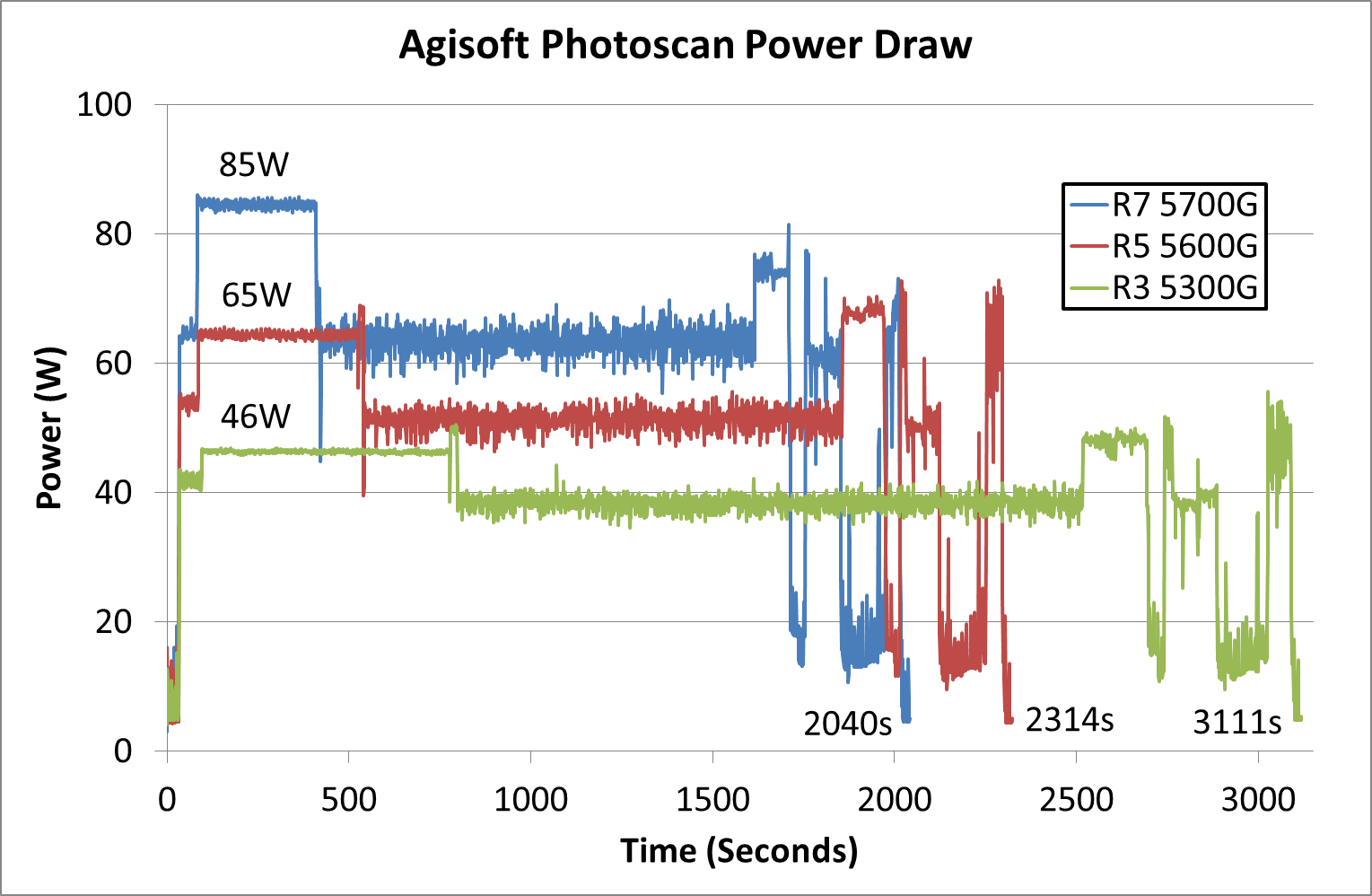
For the Ryzen 7 5700G, the most power-hungry part of the test is right at the beginning, where we’re seeing peaks of 85 W. For the 5600G, that first section goes to 65 W, but the peaks actually occur here near the end of the test. The 5300G also has peaks later in the test, but that first section is the lowest, running only at 46 W.
The second test is a sustained rendering workload.
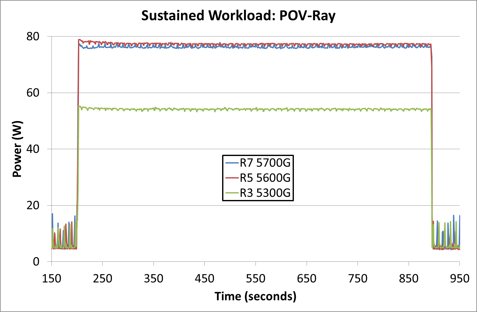
In this instance, the Ryzen 3 5300G is nearer 55 W with a sustained workload over 10 minutes, while the Ryzen 5 and Ryzen 7 sit just below 80 W.
For peak power, we report the highest value observed from any of our benchmark tests.
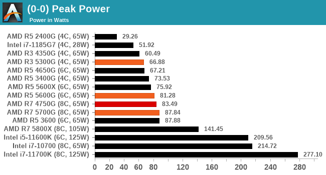
While all three processors have a TDP rating of 65 W, by default on AMD systems the Package Power Tracking, which is the limiting factor here, is 88 W. The Ryzen 7 is practically at that value, while the Ryzen 5 just goes a smidge over 80 W. The Ryzen 3 on the other hand only matches its TDP in the worst-case scenario.


135 Comments
View All Comments
abufrejoval - Thursday, August 5, 2021 - link
There are indeed so many variables and at least as many shortages these days. And it's becoming a playground for speculators, who are just looking for such fragilities in the suppy chain to extort money.I remember some Kaveri type chips being sold by AMD, which had the GPU parts chopped off by virtue of being "borderline dies" on a round 300mm wafer. Eventually they also had enough of these chips with the CPU (and SoC) portion intact, to sell them as a "GPU-less APU".
Don't know if the general layout of the dies allows for such "halflings" on the left or right of a wafer...
mode_13h - Wednesday, August 4, 2021 - link
Ian, please publish the source of 3DPM, preferably to github, gitlab, etc.mode_13h - Wednesday, August 4, 2021 - link
For me, the fact that 5600X always beats 5600G is proof that the non-APUs' lack of an on-die memory controller is no real deficiency (nor is the fact that the I/O die is fabbed on an older process node).GeoffreyA - Thursday, August 5, 2021 - link
The 5600X's bigger cache and boost could be helping it in that regard. But, yes, I don't think the on-die memory controller makes that much of a difference compared to the on-package one.mode_13h - Friday, August 6, 2021 - link
I wrote that knowing about the cache difference, but it's not going to help in all cases. If the on-die memory controller were a real benefit over having it on the I/O die, I'd expect to see at least a couple benchmarks where the 5600G outperformed the 5600X. However, they didn't switch places, even once!I know the 5600X has a higher boost clock, but they're both 65W and the G has a higher base frequency. So, even on well-threaded, non-graphical benchmarks, it's quite telling that the G can never pass the X.
GeoffreyA - Friday, August 6, 2021 - link
Remember how the Core 2 Duo left the Athlon 64 dead on the floor? And that was without an on-die MC.mode_13h - Saturday, August 7, 2021 - link
That's not relevant, since there were incredible differences in their uArch and fab nodes.In this case, we get to see Zen 3 cores on the same manufacturing process. So, it should be a very well-controlled comparison. Still not perfect, but about as close as we're going to get.
Also, the memory controller is in-package, in both cases. The main difference of concern is whether or not it's integrated into the 7 nm compute die.
GeoffreyA - Saturday, August 7, 2021 - link
In agreement with what you are saying, even in my first comment. I think Cezanne shows that having the memory controller on the package gets the critical gains (vs. the old northbridge), and going onto the main die doesn't add much more.As for K8 and Conroe, I always felt it was notable in that C2D was able to do such damage, even without an IMC. Back when K8 was the top dog, the tech press used to make a big deal about its IMC, as if there were no other improvements besides that.
mode_13h - Sunday, August 8, 2021 - link
One bad thing about moving it on-die is that this gave Intel an excuse to tie ECC memory support to the CPU, rather than just the motherboard. I had a regular Pentium 4 with ECC memory, and all it required was getting a motherboard that supported it.As I recall, the main reason Intel lagged in moving it on-die is that they were still flirting with RAMBUS, which eventually went pretty much nowhere. At work, we built one dual-CPU machine that required RAMBUS memory, but that was about the only time I touched the stuff.
As for the benefits of moving it on-die, it was seen as one of the reasons Opteron was able to pull ahead of Pentium 4. Then, when Nehalem eventually did it, it was seen as one of the reasons for its dominance over Core 2.
GeoffreyA - Sunday, August 8, 2021 - link
Intel has a fondness for technologies that go nowhere. RAMBUS was supposed to unlock the true power of the Pentium 4, whatever that meant. Well, the Willamette I used for a decade had plain SDRAM, not even DDR. But that was a downgrade, after my Athlon 64 3000+ gave up the ghost (cheapline PSU). That was DDR400. Incidentally, when the problems began, they were RAM related. Oh, those beeps!