Arm Announces Mobile Armv9 CPU Microarchitectures: Cortex-X2, Cortex-A710 & Cortex-A510
by Andrei Frumusanu on May 25, 2021 9:00 AM EST- Posted in
- SoCs
- CPUs
- Arm
- Smartphones
- Mobile
- Cortex
- ARMv9
- Cortex-X2
- Cortex-A710
- Cortex-A510
It’s that time of the year again, and after last month’s unveiling of Arm’s newest infrastructure Neoverse V1 and Neoverse N2 CPU IPs, it’s now time to cover the client and mobile side of things. This year, things Arm is shaking things up quite a bit more than usual as we’re seeing three new generation microarchitectures for mobile and client: The flagship Cortex-X2 core, a new A78 successor in the form of the Cortex-A710, and for the first time in years, a brand-new little core with the new Cortex-A510. The three new CPUs form a new trio of Armv9 compatible designs that aim to mark a larger architectural/ISA shift that comes very seldomly in the industry.
Alongside the new CPU cores, we’re also seeing a new L3 and cluster design with the DSU-110, and Arm is also making a big upgrade in its interconnect IP with the new cache coherent CI-700 mesh network and NI-700 network-on-chip IPs.
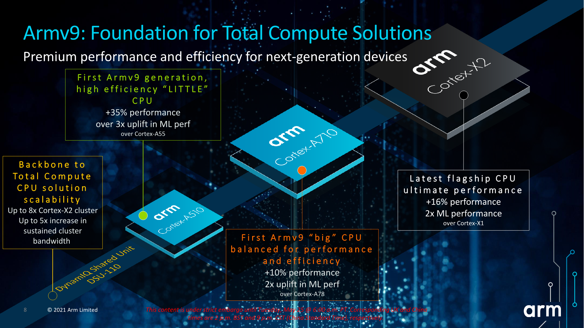
The Cortex-X2, A710 and A510 follow up on last year's X1, A78 and A55. For the new Cortex-X2 and A710 in particular, these are direct microarchitectural successors to their predecessors. These parts, while iterating on generational improvements in IPC and efficiency, also incorporate brand-new architectural features in the form of Armv9 and new extensions such as SVE2.
The Cortex-A510, Arm's new little core, is a larger microarchitectural jump, as it represents a new clean-sheet CPU design from Arm’s Cambridge CPU design team. A510 brings large IPC improvements while still having a continued focus on power efficiency, and, perhaps most interestingly, retains its characteristic in-order microarchitectural.
An Armv9 CPU Family – AArch64 only for all practical purposes*
The new CPU family marks one of the largest architectural jumps we’ve had in years, as the company is now baselining all three new CPU IPs on Armv9.0. We've extensively covered the details of the new Arm architecture back in late March. Cornerstone features of the new ISA include the new enrollment of prior optional/missing Armv8.2+ features that weren’t guaranteed in mobile and client designs (mostly due to the older A55 cores), and the introduction of new SVE2 SIMD and vector extensions.
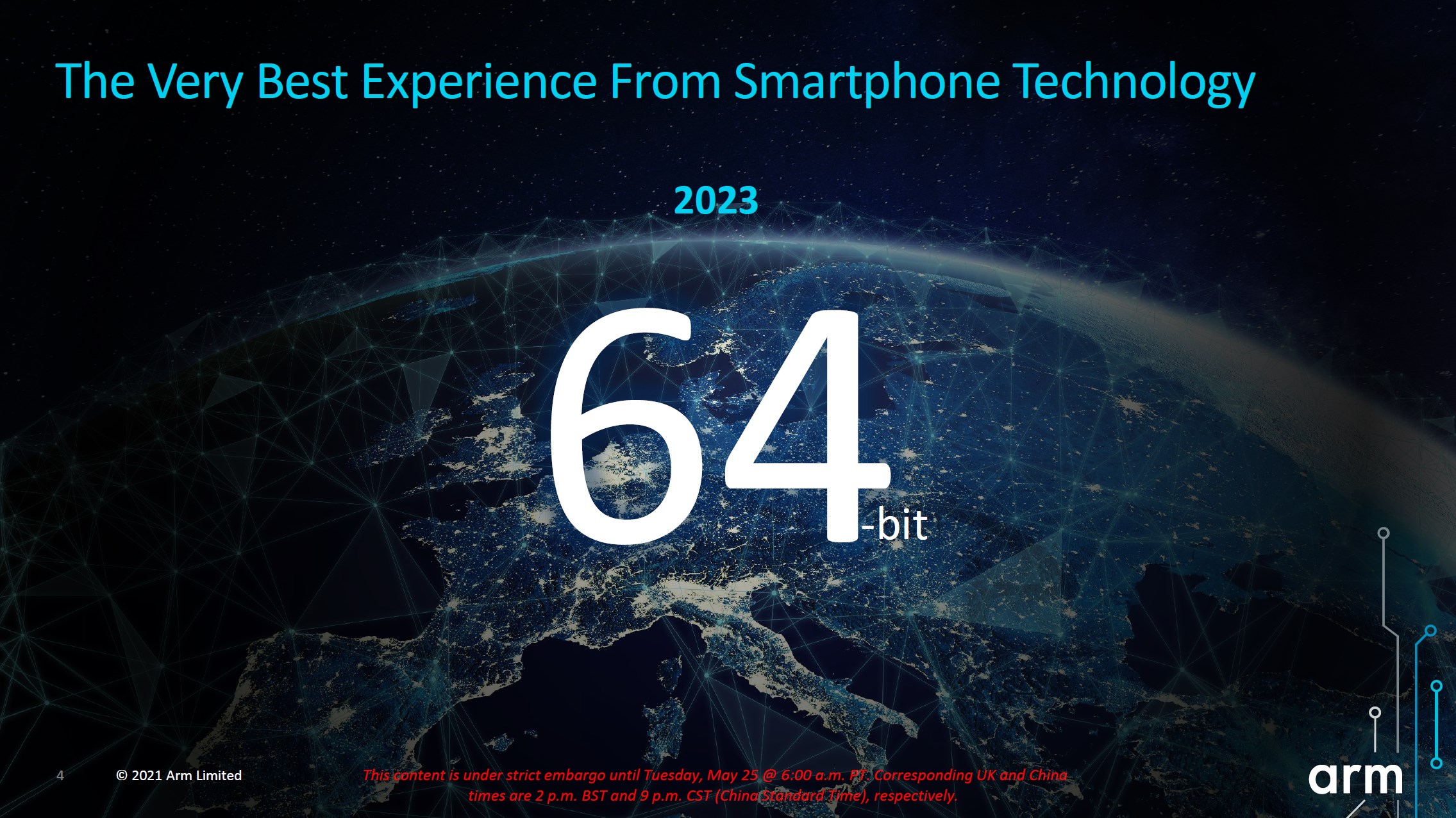
One big change we’ve been expecting for quite some time now is that we’ll be seeing a deprecation of the 32-bit AArch32 execution mode in upcoming Arm Cortex-A mobile cores. The clock has been ticking for 32-bit apps ever since Google’s announced in 2019 that the Google Play store will require for 64-bit app uploads, and the company will stop serving 32-bit applications to 64-bit compatible devices later this summer
While Arm is declaring that shift to happen in 2023, for all intents and purposes it’s already happening next year for most global users. Both the Cortex-X2 flagship core and the Cortex-A510 little cores are AArch64-only microarchitectures that are no longer able to execute AArch32 code.
With that said, sharp readers will note that two out of three CPUs isn't a complete shift, and the reason for that is because the Cortex-A710 actually still supports AArch32. Arm states that the reason for this is primarily to meet the needs of the Chinese mobile market, which lacks the homogeneous ecosystem capabilities of the global Play Store markets, and Chinese vendors and their domestic app market require a little more time to facilitate the shift towards 64-bit only. This means we’ll have an odd scenario next year of having SoCs on which only the middle cores are able to execute 32-bit applications, with those apps being relegated to the middle A710 cores and missing out on the little A510 cores’ power efficiency or the X2 cores’ performance.
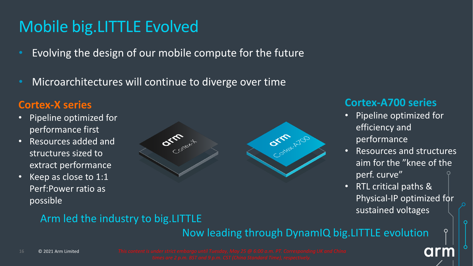
On the big core side, the new Cortex-X2 and Cortex-A710 are successors to the Cortex-X1 and Cortex-A78. Both designs are mostly designed by Arm’s Austin design team, and represent the 4th generation of this microarchitecture family, which had started off with the Cortex-A76 several years ago. These cores should be the last of this microarchitecture family before Arm hands things off to a completely new design with next year’s new Sophia cores.
In terms of design philosophy, the X2 and A710 generally keep the same overarching goals the X1 and A78 had defined: The X-series continues to focus on advancing performance by increasing microarchitectural structures and by Arm being willing to make compromises on power within reasonable limits. Meanwhile the A710 continues to focus on advancing performance and efficiency through smarter design and with a large focus on maximizing the power, performance, and area (PPA) balance of the IP.
One point Arm makes in the above slide is having optimized critical paths and physical design for sustained voltage operations – this is more of a goal the company is striving for in the next generations of “middle” cores rather than something that’s specifically reflected in the Cortex-A710.
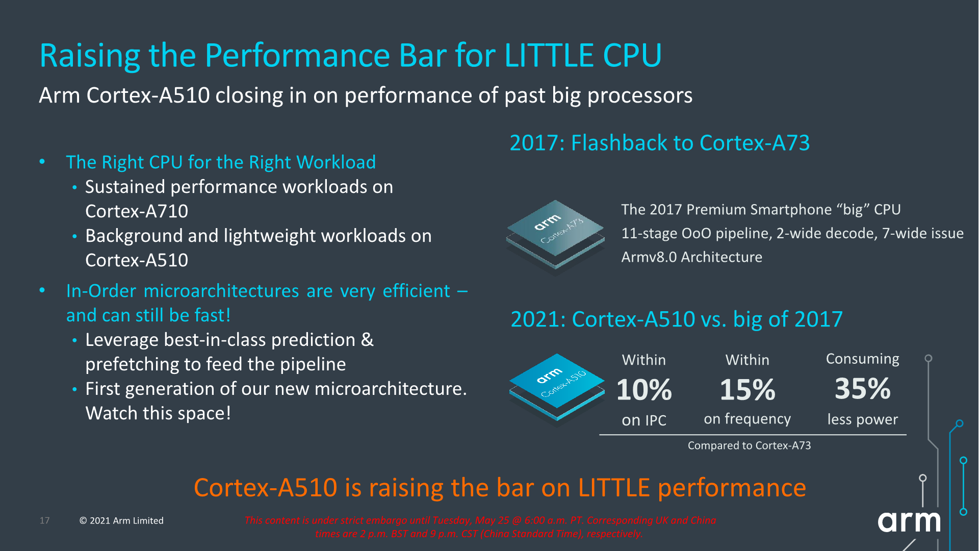
This year, we are also finally seeing a new little core. We had covered the Cortex-A55 back in 2017, and since then we haven’t had seen any updates to Arm’s little cores, to the point of it being seen as large weakness of last few generations of mobile SoCs.
The new Cortex-A510 is a clean-sheet design from Arm’s Cambridge design team, leveraging a lot of the technologies that had been employed in the company’s larger cores, but implemented into a new in-order little microarchitecture. Yes – we’re still talking about an in-order core, and Arm still sees this to be the best choice in terms of extracting the best efficiency and “Days of use” of mobile devices.
Even though it’s a in-order core, Arm made a comparison that the new design is extremely similar to a flagship core of 2017 – namely the Cortex-A73, achieving very similar IPC and frequency capabilities whilst consuming a lot less power.
The new design also comes with a very interesting shared complex approach and shares the L2 and FP/SIMD pipelines with a second core, a design approach Arm calls “merged core” and undoubtedly will remind readers of AMD’s CMT approach in Bulldozer cores 10 years ago, even though there are quite important differences in the approaches.


181 Comments
View All Comments
ChrisGX - Thursday, May 27, 2021 - link
Using Andrei's initial performance estimate for the X1 (clocked at 3GHz) as a guide (47.2 SPECint2006) and ARM's own projection for the peak performance boost offered by the X2 over the X1 (+30% when process optimisations and frequency increases are factored in) we get a rating of 61.4 SPECint2006 for next years X series core. That is really a best case estimate and it is where the good news ends.The information we have on the 2022 Cortex cores does seem to lack the transparency of material of this sort that had been issued in earlier years by ARM. It is disappointing not to have any core frequency data in that information. A lot turns on realistic estimations of attainable core frequencies and having a good sense of power dissipation at maximum burst frequencies. We now know that Andrei's performance estimate for the X1 core wasn't borne out in practice (the actual performance exhibited by the highest performing X1 core - the one in the Snapdragon 888 - was 14% lower at 41.3 SPECint2006) owing to pitiful power dissipation characteristics of Samsung's 5nm LPE process that in order to prevent thermal build up and keep power consumption within budget on SoCs incorporating an X1 core SoC designers found it necessary to either a) reduce burst clock frequencies to below 3GHz or b) use restrictive power management controls to damp down chip operations threatening the thermal stability of the SoC that will naturally have the effect of throttling performance.
Using more realistic assumptions to project the likely performance of the X2 core (which I suspect might still be too optimistic because these forthcoming SoCs that incorporate an X2 core like the flagship Android smartphone SoCs of 2021 are said to be scheduled for production on Samsung fabs which must cast a degree of doubt on ARM's performance projections because recently Samsung's silicon process technologies have demonstrably failed to come up tp ARM's expectations) we get this number: 53.7 SPECint2006 (which represents the actual performance of the highest performing X1 core of 2021 x 1.3). Given the lack of transparency in the ARM data it is possible to entertain a rather broad range of imaginable SPEC peak integer performance ratings for the X2 core. A SPECspeed of 53.7 is my best guess.
ikjadoon - Tuesday, May 25, 2021 - link
These are geometric means of integer & FP scores. Typo for X1, ~50 not ~40. Let's be precise, now that I'm not on a phone ;)SPEC2006 1T Geomean:
A14 Firestorm = 71.72 points
A13 Lightning = 59.09 points
SD888 X1 = 49.48 points
Awarding the X2 the full 16% jump on both integer & FP, we can napkin math this to a Reference X2 = 57.40 at iso-frequency.
You're right they can (and maybe should) boost clocks so it could surpass the A13, but it's unrealistic to imagine Qualcomm shipping a 3.3+ GHz smartphone in 2022, especially if it's Samsung foundries again, but even on TSMC. Qualcomm's SD888 X1 at 2.84 GHz already ate 9621 joules (SPECint2006) and 4972 joules (SPECfp2006).
From https://www.anandtech.com/show/16463/snapdragon-88...
No one expects a literal doubling, but Arm's competition (NUVIA, Apple, Ampere) are not slowing down, either.
Wilco1 - Tuesday, May 25, 2021 - link
OK I get it now - the 40 made me think you meant SPECINT as that is what Cortex-X1 scored.3.3GHz on TSMC 5nm is conservative given it has significant performance/power improvements (which the A14 already benefits from), but yes it means switching back to TSMC.
Thala - Tuesday, May 25, 2021 - link
Indeed the performance gains of A14 vs. A13 are mostly frequency driven and much less IPC driven. It is not unreasonable to assume some frequency gains for X2 as well when moving to 5nm TSMC.Ppietra - Wednesday, May 26, 2021 - link
Thala, looking at the numbers IPC improved 8%, being responsible for 42% of performance growth... so not exactly much less!A13 to A14 transition gives no clue about what would happen between X1 and X2 or between Samsung and TSMC... X1 is already at 5nm, and its clock speed is just 5% less than the A14... Their designs priorities are also different, so you cannot infer much!
name99 - Tuesday, May 25, 2021 - link
All true. But of course A14 is an especially easy opponent!- it's the last round of what appears to be Apple's 4-year "seriously new micro-architecture" cadence -- A77..A10 as gen 1, A11..A14 as gen 2, A15 et seq as gen 3.
- it was clearly designed with the single highest priority being get the x86 stuff working. Meaning that anything that did not match that priority (including, eg, optimized physical layout and risky micro-architectural innovations) was punted till the A15
- it doesn't have SVE/2, which is good for anything up to a 80% speed boost depending on the exact code (even with just compiler vectorization). Averaging over "representative code bases" is a game that's never going to get everyone to agree, but the one attempt I saw to do this came up with an average performance boost of ~30%.
Given how *low* ARM's numbers are, I assume they're talking about performance in the absence of use of SVE/2? Honestly the whole thing is kinda weird, how little they're pushing the SVE/2 angle and how much one might expect it to improve things.
I do *not* expect Apple to be as timid... And while Apple tend to shy away from hardware announcements at WWDC, we all know about M1 by now, AND we know that SVE/2 will be in next year's ARM (so presumably in this year's Apple). Meaning maybe there will be some talks about SVE/2 (and other ARMv9 stuff) at WWDC?
Wilco1 - Tuesday, May 25, 2021 - link
You are exaggerating the gains of SIMD in general. Yes automatic vectorization helps, but even if it improves some image transformations by 80%, it's never going to speed up browsing by 30%. Or any other general purpose code. Or SPEC.Remember this is 128-bit SVE, so 4 Neon units are about as fast as 4 SVE units. For great SVE performance on HPC code look at A64FX or the upcoming Neoverse V1.
name99 - Tuesday, May 25, 2021 - link
- One hopes that the combination of agnostic length and predicates will allow a lot of code for which vectorization was previously uneconomical (too expensive to mask out fiddly bits, too much overhead in loop prologs and epilogs) to now be handled. We shall see.- You are right about the 128b of course; yet another instance of ARM never trying for a stretch goal! I assume Apple will be implementing this as 2x256, meaning, among other things, the path from L1D to LSU grows from 128b to 256b wide, and that's an example of where SVE/2 (indirectly, sure) helps boost performance for everyone.
smalM - Friday, May 28, 2021 - link
Could you please explain why you asume Apple will reduce the number of FP/SIMD units in exchange for widening them. Is that really better? From a FP or from a SIMD standpoint?Thanks in advance.
Making the path from L1D to LSU 256b wide is something Apple could do anyways and is not directly related to SVE2; I was astonished they didn't do it when they added the fourth FP/NEON unit.
mode_13h - Saturday, May 29, 2021 - link
> would you please explain why you asume Apple will reduce the number of FP/SIMD units> in exchange for widening them. Is that really better?
For SVE it's a little better, since it means software having to run loops for about half as many iterations, correspondingly reducing loop overhead.
> Making the path from L1D to LSU 256b wide is something Apple could
> do anyways and is not directly related to SVE2
I don't really see why. It seems like it'd only help for back-to-back reads or writes from/to consecutive addresses. And if 128-bits is already enough to do that, then extra width would be a waste.