The Ampere Altra Review: 2x 80 Cores Arm Server Performance Monster
by Andrei Frumusanu on December 18, 2020 6:00 AM EST- Posted in
- Servers
- Neoverse N1
- Ampere
- Altra
As we’re wrapping up 2020, one last large review item for the year is Ampere’s long promised new Altra Arm server processor. This year has indeed been the year where Arm servers have had a breakthrough; Arm’s new Neoverse-N1 CPU core had been the IP designer’s first true dedicated server core, promising focused performance and efficiency for the datacentre.
Earlier in the year we had the chance to test out the first Neoverse-N1 silicon in the form of Amazon’s Graviton2 inside of AWS EC2 cloud compute offering. The Graviton2 seemed like a very impressive design, but was rather conservative in its goals, and it’s also a piece of hardware that the general public cannot access outside of Amazon’s own cloud services.
Ampere Computing, founded in 2017 by former Intel president Renée James, built upon initial IP and design talent of AppliedMicro’s X-Gene CPUs, and with Arm Holdings becoming an investor in 2019, is at this moment in time the sole “true” merchant silicon vendor designing and offering up Neoverse-N1 server designs.
To date, the company has had a few products out in the form of the eMAG chips, but with rather disappointing performance figures - understandable given that those were essentially legacy products based on the old X-Gene microarchitecture.
Ampere’s new Altra product line, on the other hand is the culmination of several years of work and close collaboration with Arm – and the company first “true” product which can be viewed as Ampere pedigree.
Today, with hardware in hand, we’re finally taking a look at the very first publicly available high-performance Neoverse based Arm server hardware, designed for nothing less than maximum achievable performance, aiming to battle the best designs from Intel and AMD.
Mount Jade Server with Altra Quicksilver
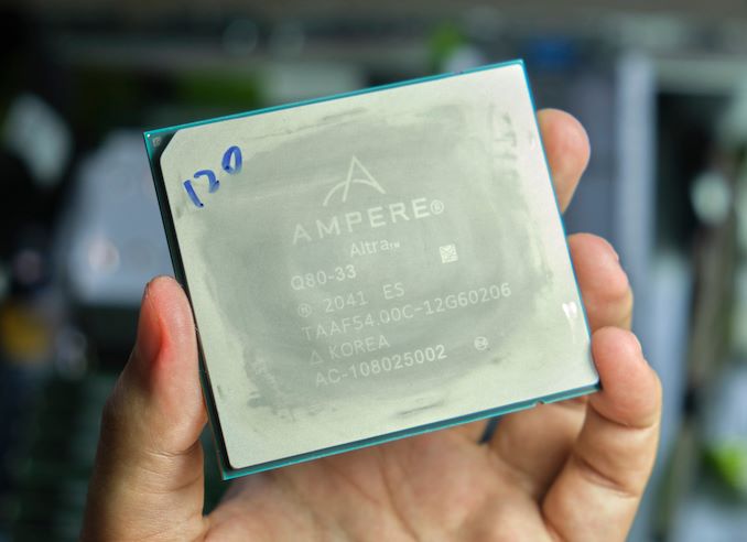
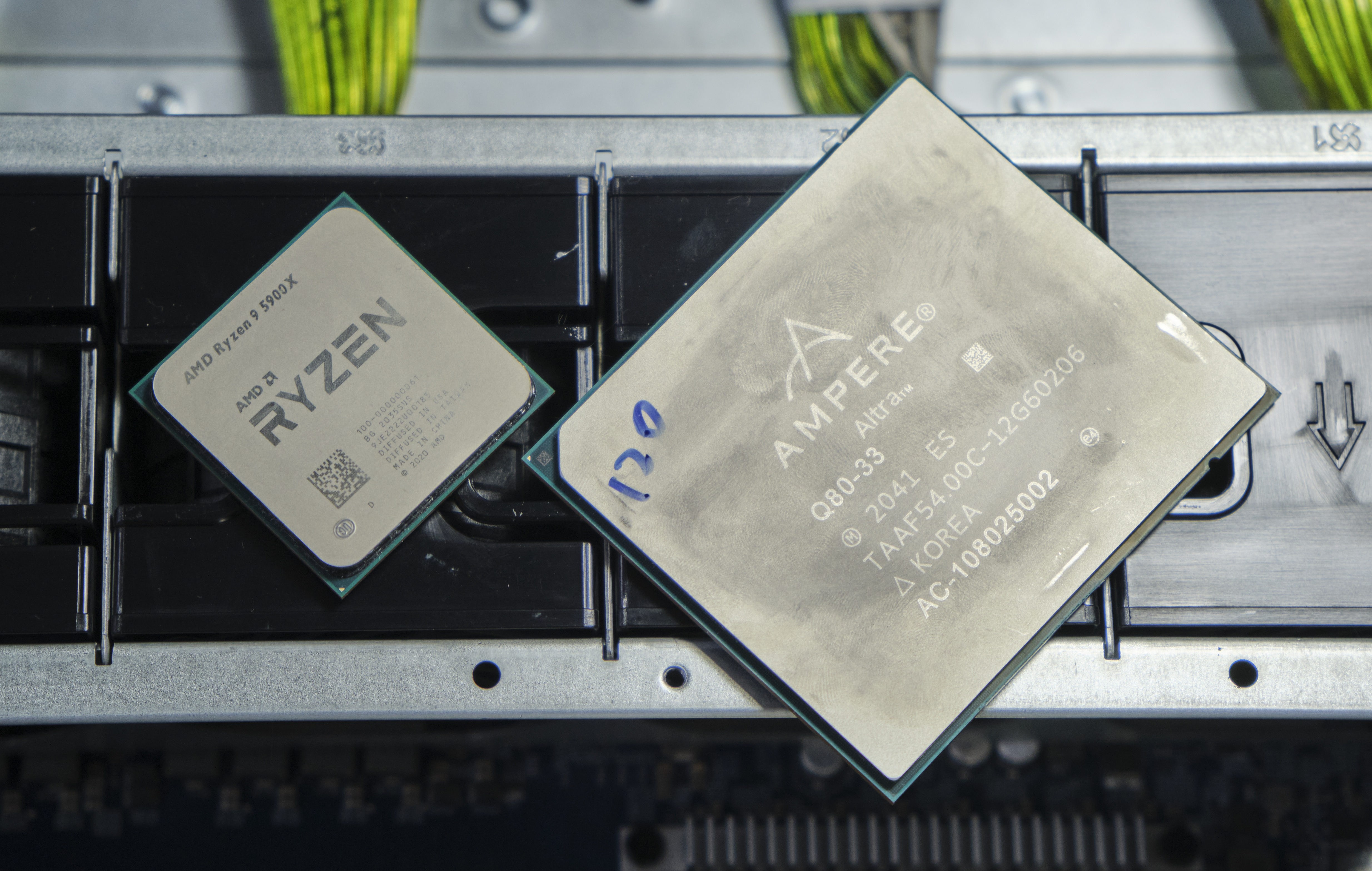
Ampere has supplied us with the company’s server reference design, dubbed “Mount Jade”, a 2-socket 2U rack unit sever. The server came supplied with two Altra Q80-33 processors, Ampere’s top-of-the-line SKU with each featuring 80 cores running at up to 3.3GHz, with TDP reaching up to 250W per socket.
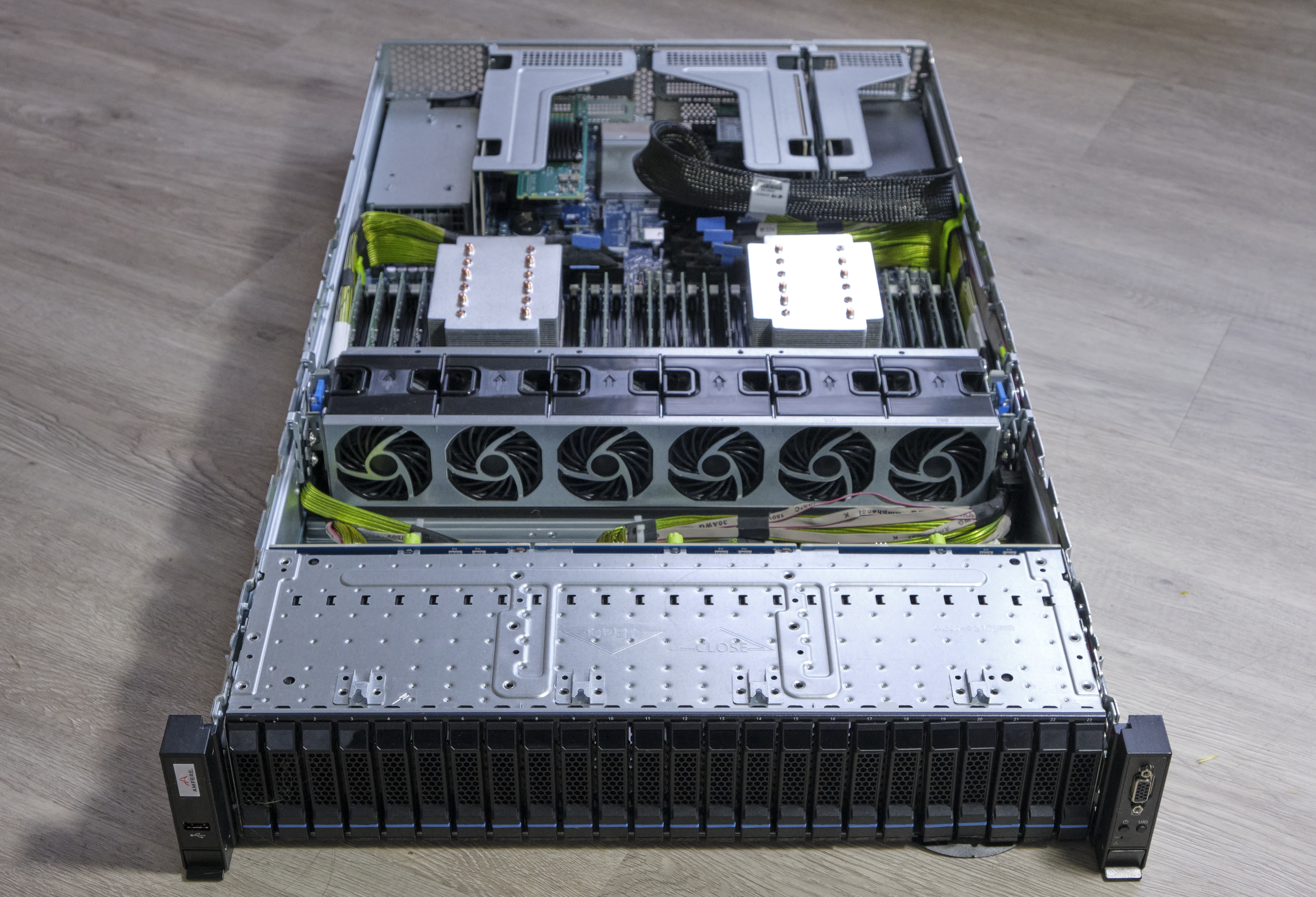
The server was designed with close collaboration with Wiwynn for this dual socket, and with GIGABYTE for the single socket variant, as previously hinted by the two company’s announcements of leading hyperscale deployments of the Altra platforms. The Ampere-branded Mount Jade DVT reference motherboard comes in a typical server blue colour scheme and features 2 sockets with up to 16 DIMM slots per socket, reaching up to 4TB DRAM capacity per socket, although our review unit came equipped with 256GB per socket across 8 DIMMs to fully populate the chip’s 8-channel memory controllers.
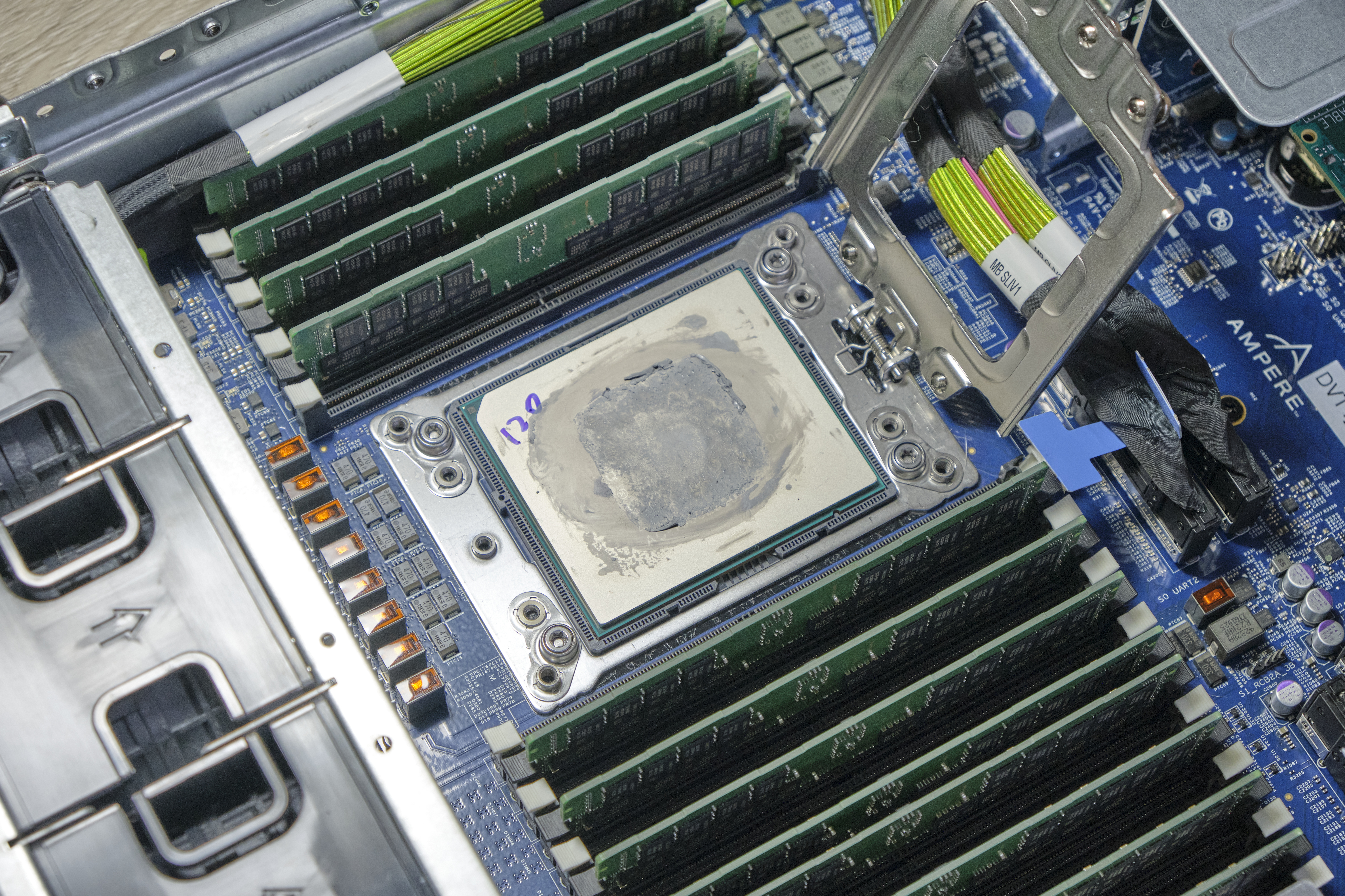
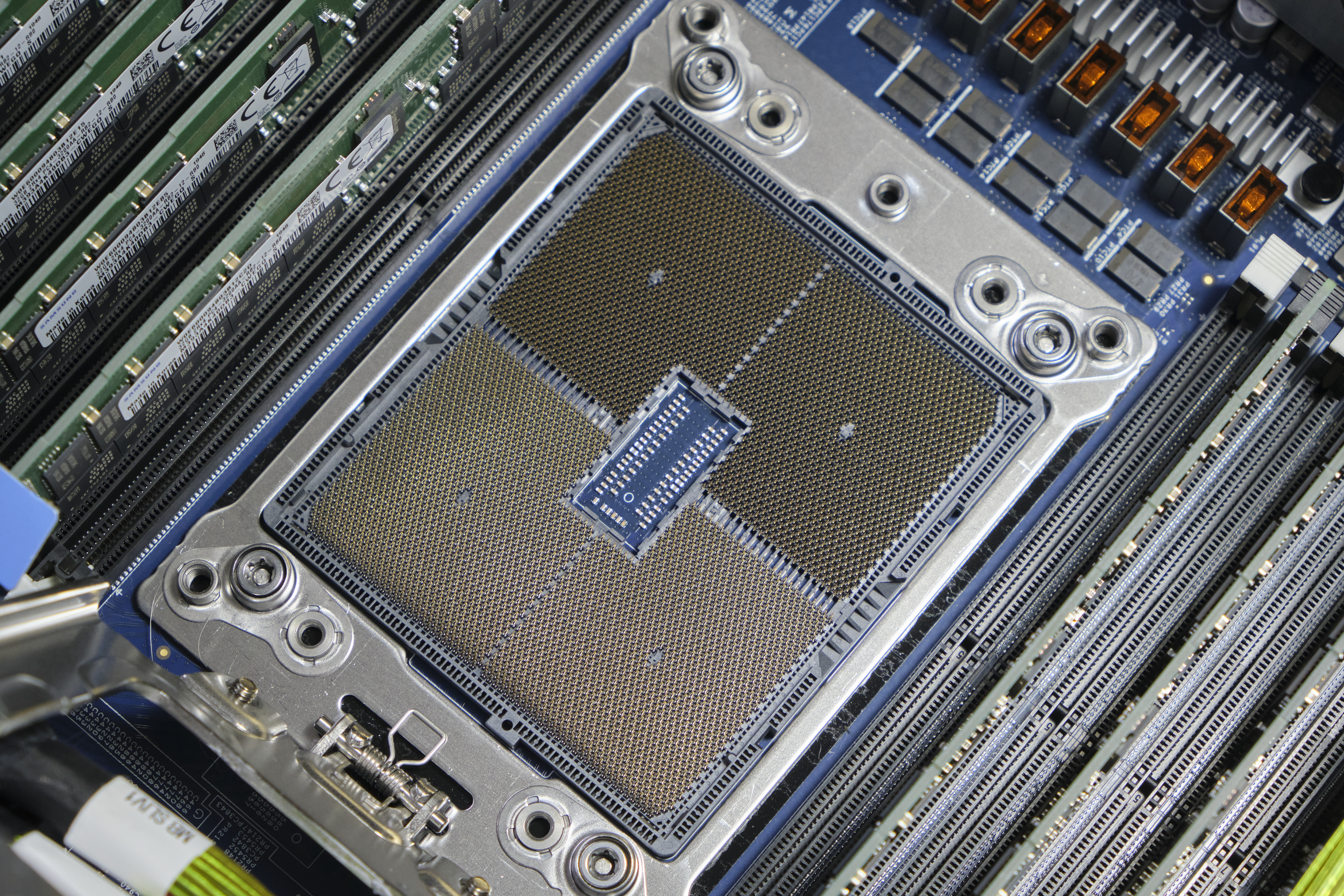
This is also our first look at Ampere’s first-generation socket design. The company doesn’t really market any particular name to the socket, but it’s a massive LGA4926 socket with a pin-count in excess of any other commercial server socket from AMD or Intel. The holding mechanism is somewhat similar to that of AMD’s SP3 system, with a holding mechanism tensioned by a 5-point screw system.
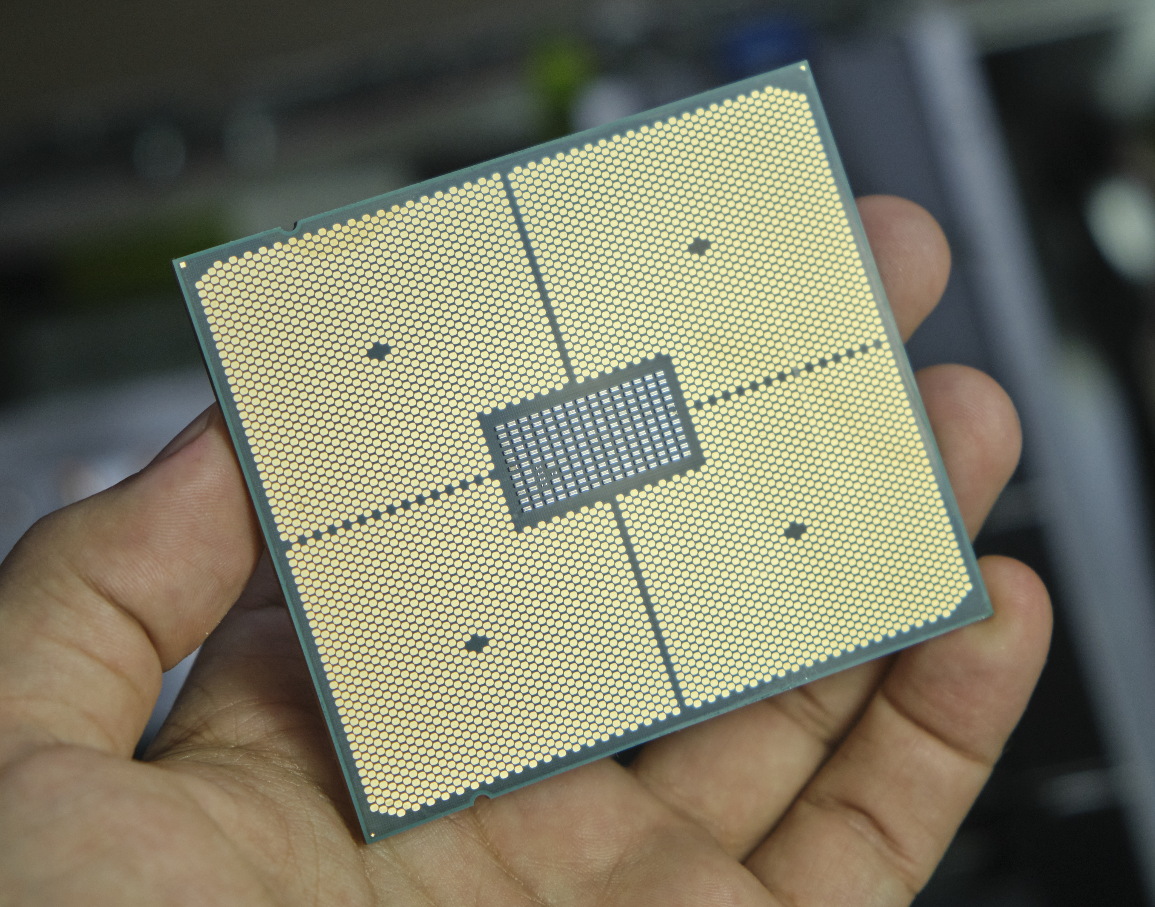
The chip itself is absolutely humongous and amongst the current publicly available processors is the biggest in the industry, out-sizing AMD’s SP3 form-factor packaging, coming in at around 77 x 66.8mm – about the same length but considerably wider than AMD’s counterparts.
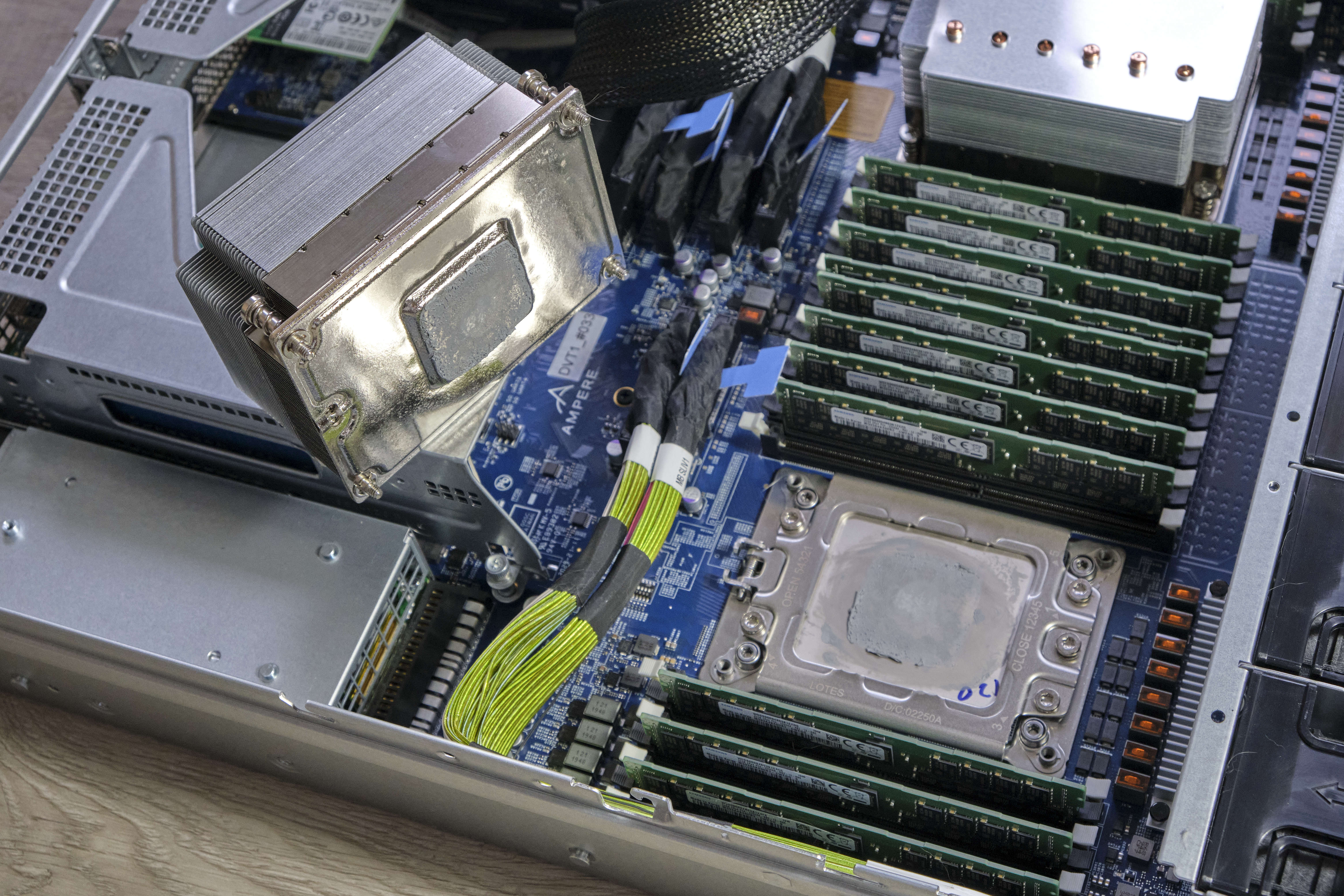
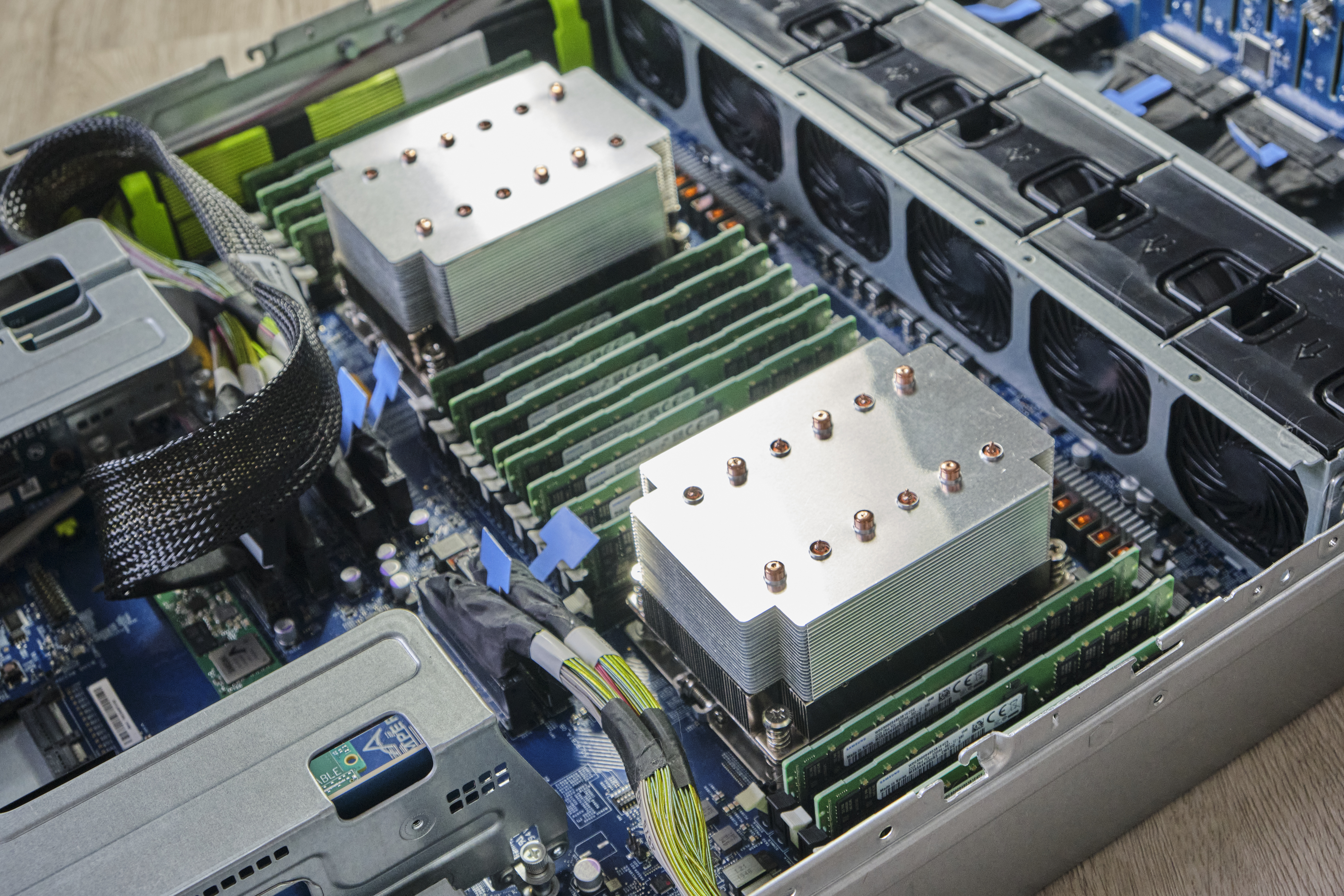
Although it’s a massive chip with a huge IHS, the Mount Jade server surprised me with its cooling solution as the included 250W type cooler only made contact with about 1/4th the surface area of the heat spreader.
Ampere here doesn’t have a recessed “lip” around the IHS for the mounting bracket to hold onto the chip like on AMD or Intel systems, so the actual IHS surface is actually recessed in relation to the bracket which means you cannot have a flat surface cooler design across the whole of the chip surface.

Instead, the included 250W design cooler uses a huge vapour chamber design with a “pedestal” to make contact with the chip. Ampere explains that they’ve experimented with different designs and found that a smaller area pedestal actually worked better for heat dissipation – siphoning heat off from the actual chip die which is notably smaller than the IHS and chip package.
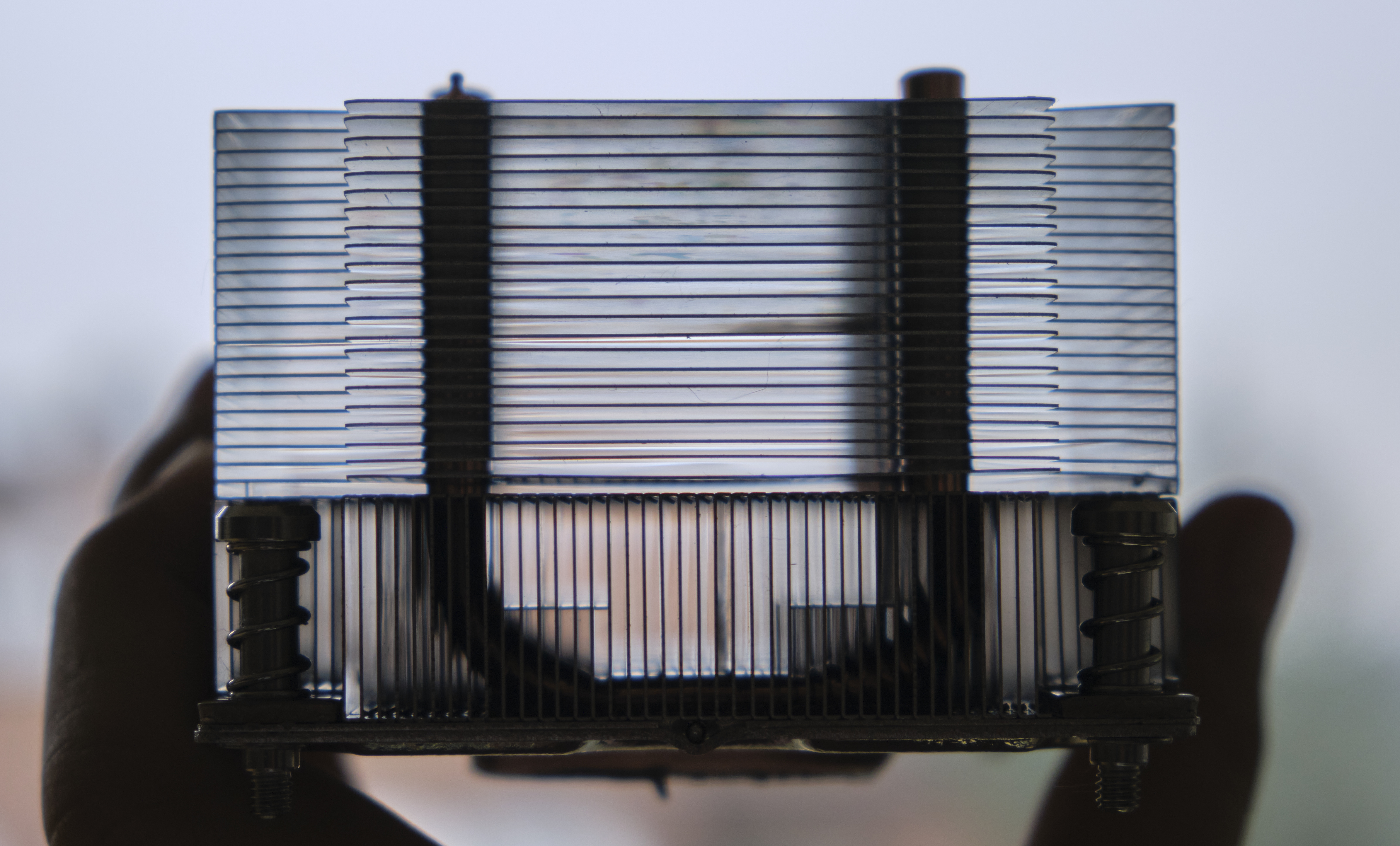
The cooler design is quite complex, with vertical fin stacks dissipating heat directly off the vapour chamber, with additional large horizontal fins dissipating heat from 6 U-shaped heat pipes that draw heat from the vapour chamber. It’s definitely a more complex and high-end design than what we’re used to in server coolers.
Although the Mount Jade server is definitely a very interesting piece of hardware, our focus today lies around the actual new Altra processors themselves, so let’s dive into the new Q80-33 80-core chip next.


148 Comments
View All Comments
Wilco1 - Friday, December 18, 2020 - link
How exactly is it big? It's tiny for a server chip - 80 cores at about half the die size of a typical 28-core Xeon (~700mm^2). And TSMC 7nm yield is extremely good even for much larger chips like GPUs.Ithaqua - Friday, December 18, 2020 - link
Plus as with all chips, there may be a 64 / 48 / 32 core version which are just standard chips with the defective core block turned off.eastcoast_pete - Saturday, December 19, 2020 - link
Note I wrote "quite big", and by transistor count, it's a larger CPU, expected for a server chip. As for the Xeon, how high is Intel's yield for the 28 core Xeon, and that after how many years on 14 nm+++ (etc)? So, if you have a yield number for this 80 core Ampere chip, please share it.Wilco1 - Saturday, December 19, 2020 - link
It's larger than a mobile SoC, but small for a server chip thanks to Arm's tiny cores and the high density of TSMC 7nm. See https://www.anandtech.com/show/16028/better-yield-... for the defect rate, and from that a simple yield calculator gives 71% for a 350mm^2 die. That's before you fix SRAM defects or harvest dies for the lower-end SKUs. So we conclude yield is very good.eastcoast_pete - Saturday, December 19, 2020 - link
Glad to read that you've proven Andrei wrong, so maybe you should write these reviews. Here a direct quote from the first page of the review (also, take a look at the pictures: "The chip itself is absolutely humongous and amongst the current publicly available processors is the biggest in the industry, out-sizing AMD’s SP3 form-factor packaging, coming in at around 77 x 66.8mm – about the same length but considerably wider than AMD’s counterparts."Wilco1 - Saturday, December 19, 2020 - link
How ignorant can you be? Obviously the chip and silicon die have different sizes. The chip is large because it has many pins. The silicon die is a tiny fraction of the chip. We're discussing the size of the silicon die here, not the size of the chip. Completely different things.mode_13h - Sunday, December 20, 2020 - link
It'd be less confusing if you'd talk about the "package" dimensions.I think die and chip are traditionally synonymous. For instance, a package with multiple dies is traditionally called a MCM (Multi-Chip Module).
Wilco1 - Monday, December 21, 2020 - link
Look at Andrei's quote above, there isn't a well-defined term - people use chip/CPU/package etc as synonyms.mode_13h - Monday, December 21, 2020 - link
But it's not hard to see how "chip" can cause confusion. So, why not avoid it entirely, and just say either "die" or "package".Only a troll or someone with an agenda could be against clear communication.
Wilco1 - Monday, December 21, 2020 - link
It's hard to imagine how anyone sane can believe that a "chip measuring 77 x 66.8mm" (6 times the reticle limit!) is referring to the die size rather than the package. Andrei's quote even uses the word package. So maybe you're right and eastcoast_pete was just trolling.