Where are my GAA-FETs? TSMC to Stay with FinFET for 3nm
by Dr. Ian Cutress on August 26, 2020 12:00 PM EST
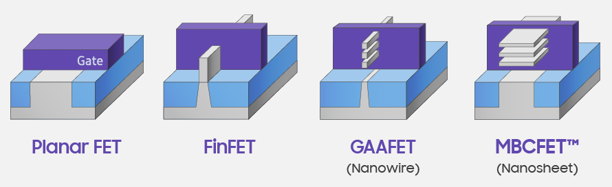
As we passed that 22nm to 16nm barrier, almost all the major semiconductor fabrication companies on the leading edge transitioned from planar transistors to FinFET transistors. The benefits of FinFET were numerous, including better drive currents and lower leakage, better scalability, faster switching times, and an overall better transistor of choice for semiconductor logic. With FinFETs, and multiple rounds of improvements, the technology has scaled from Intel’s first 22nm products down to the 5nm products we will see from TSMC’s partners this year.
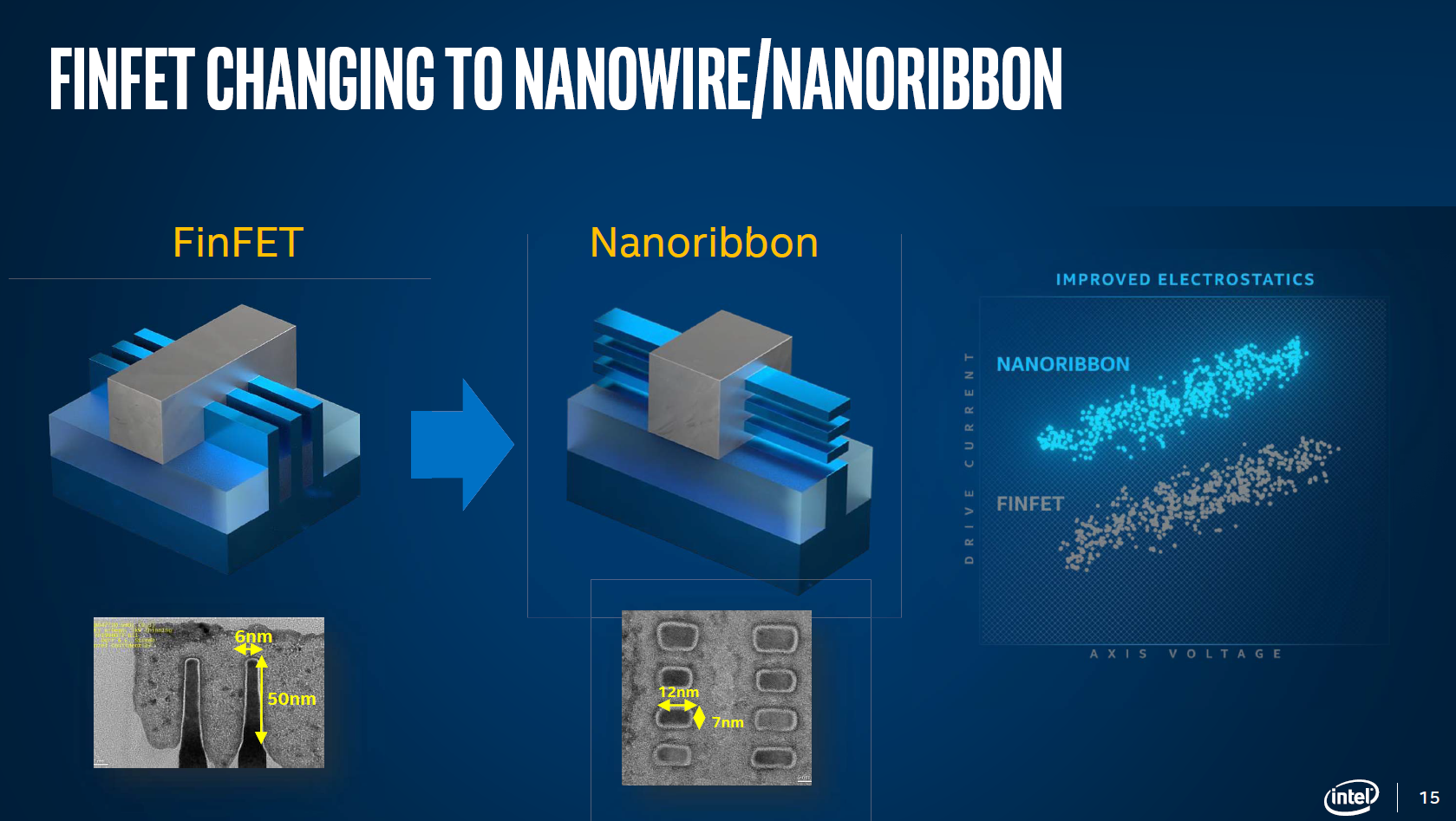
As expected, at some point the ability to scale a FinFET will become prohibitive, and new technologies will be needed to help continue the scaling. Research on post-FinFET transistor technology has been progressing at a break-neck pace, and most attention has been moved into ‘Gate-All-Around’ technology, which lifts the channel and allows the channel width to scale as needed for the type of transistor in use. GAA-FETs offer significant advantages when it comes to transistor performance control – for most FinFET processes, foundries can offer several designs based on voltage and performance, but GAA-FET designs turn those discrete options into something more continuous. You might see these referred to as nanosheets, or nanowires.
From Samsung
As is perhaps to be expected, GAA-FET designs (and layered GAA-FETs) are more complex to build than FinFETs or planar transistors. The first GAA-FET demonstration was in 1986, and in 2006 a 3nm implementation was demonstrated. However, building it in a lab compared to building it at scale as part of a foundry process available to customers is a different scale of complexity. At a number of technical semiconductor conferences through 2018 and 2019, a number of design companies and foundry offerings have discussed GAA-FET or similar designs as part of their upcoming portfolio.
Most notably, Intel has mentioned that they will start using it within the next 5 years, which would put it around its 5nm-3nm node technologies.
Intel
Samsung has announced its intention to deliver its version, known as MBC-FETs, as part of its 3nm process node, expected to be in volume manufacturing by late 2021. In May 2019, the company released a statement that the first v0.1 version of its 3GAE PDK was ready for customers. Over a year later, we would expect this to be on track – the 2020 version of Samsung’s Foundry Forum, which was delayed due to COVID, should be happening later this year.

Samsung
As these sorts of transistors grow in use, we expect the range of sheet widths available to increase, as well as the number of stacked layers in a GAA design. CEA-Leti this year, at the 2020 Symposia on VLSI Technology and Circuits, demonstrated a 7-layer GAA-FET using nanosheets specifically for high-performance computing.
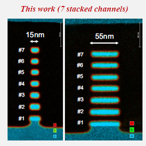
CEA-Leti
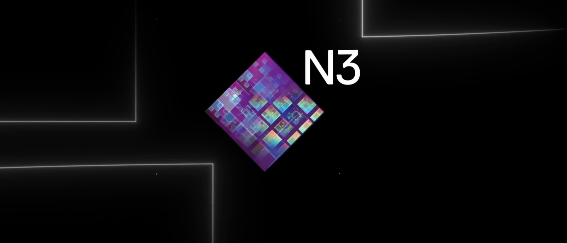
So what has happened with TSMC? As part of the Technology Symposium, it has stated that for its 3nm process technology it will remain with FinFETs. The company states that it has enabled a significant update to its FinFET technology to allow performance and leakage scaling through another iteration of its process node technology. TSMC’s N3 will use an extended and improved version on FinFET in order to extract additional PPA - up to 50% performance gain, up to 30% power reduction, and 1.7x density gain over N5. TSMC stated the predictability of FinFETs will help enable the company deliver the technology on an approved timescale.
This last statement is more than telling – if the development of FinFETs, now on its 3rd/4th/5th generation (depending on the foundry), has enabled a level of comfort and predictability that a first generation of GAA-FET cannot provide, then in order to satisfy its big customers (almost all leading-edge logic silicon), it has to keep to its cadence. That being said, there could be a chance for TSMC to offer GAA-FETs on different versions of its 3nm nodes in the future if it wishes, however the company has not made any public statements at this time to this effect, compared to Intel and Samsung.
As always with these technologies, the goal is to scale and bring some reality to wherever Moore’s Law is going. TSMC’s customers will have to wait until later to see if GAA-FETs can bring a more optimized flavor of performance to the table.
Related Reading
- TSMC Details 3nm Process Technology: Full Node Scaling for 2H22 Volume Production
- TSMC To Build 5nm Fab In Arizona, Set To Come Online In 2024
- TSMC & Broadcom Develop 1,700 mm2 CoWoS Interposer: 2X Larger Than Reticles
- TSMC Boosts CapEx by $1 Billion, Expects N5 Node to Be Major Success
- Early TSMC 5nm Test Chip Yields 80%, HVM Coming in H1 2020
- TSMC: 5nm on Track for Q2 2020 HVM, Will Ramp Faster Than 7nm
- TSMC: N7+ EUV Process Technology in High Volume, 6nm (N6) Coming Soon


37 Comments
View All Comments
drexnx - Wednesday, August 26, 2020 - link
wonder if they'll go to .x nanometer first like they did with micron before finally going to nanometer at the 90nm node. Back then it was weird to see something you'd always seen before as .13u == 130nmEliadbu - Wednesday, August 26, 2020 - link
Back than the process name had something to do with the some of the transistor feature size, today it has nothing to do with with any size or density, So they can call the process unicorns and rainbows - not likex nm has to do more with the process.
Spunjji - Thursday, August 27, 2020 - link
It really does have a lot to do with the density, though. The density has been improving at roughly the same rate as the name changes would imply.Spunjji - Thursday, August 27, 2020 - link
To be clear - the transistor sizes aren't accurately represented, but the differences between processes largely are. That seems to be the point of the exercise.Arsenica - Wednesday, August 26, 2020 - link
3 nm is 3000 pm.Angstroms would be a more marketable term ( 3 nm is 30 Å), but pretty much no component of a transistor would measure that as stochastics in that scale would kill the yields of anybody trying to actually reach Angstroms. Hell, stochastics are currently killing the yields of Intel's "copy-exact" methodology at 7 "nm".
In a few years TSMC could likely announce their Å20 gate-all-around process featuring eh.. 15 nm gate ribbon/sheet widths.
FunBunny2 - Wednesday, August 26, 2020 - link
in due time, these transistors with be Heisenberg devices, except not under humans' control.quorm - Wednesday, August 26, 2020 - link
0.3nm / 300 pm is unlikely to ever happen, unless the correspondence between node naming and transistor size becomes even less meaningful.Slumberthud - Wednesday, August 26, 2020 - link
Except that 3 nm is 3000 pm, not 300 pm.astroboy888 - Thursday, August 27, 2020 - link
Or angstrom. which is 1e-10. :) 1nm would be 10 angstrom.3nano-meter is 3000 pico-meter.
boeush - Friday, August 28, 2020 - link
Keep in mind that the diameter of a single Silicon atom is 0.222 nm (at room temperature, I believe) - which is 222 pm. Thus it's physically impossible for a transistor to be smaller than that, at least.Worse, if one considers the Si crystal lattice, then a single unit of the cubic lattice is about 0.543 nm on its side. This is probably the irreducible size quantum for Si-based circuitry, since at fractions of this you might wind up with a chemically-unstable structure.
But in reality, it's unlikely that transistors will ever shrink to the size of a single Si atom, or even a single unit of Si crystal lattice. If one assumes let's say 3 lattice units in terms of nanowire/nanosheet width for end-state transistor tech, then the absolute size limit for the 'smallest feature' would be around 1.63 nm or so. It's probably safe to assume anything beyond that would be solidly in the realm of fantasy.
Of course, 'smallest feature' in this case will have little in common with the size of an actual transistor (including any spacing required between it and adjacent transitors to suppress electromagnetic cross-talk.)