TSMC Details 3nm Process Technology: Full Node Scaling for 2H22 Volume Production
by Andrei Frumusanu on August 24, 2020 3:30 PM EST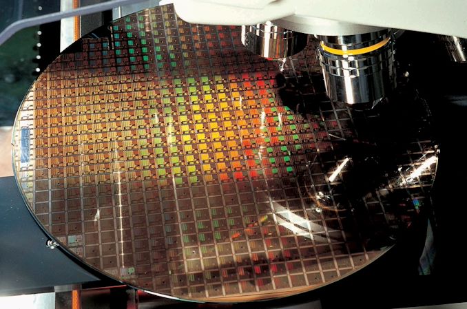
At TSMC’s annual Technology Symposium, the Taiwanese semiconductor manufacturer detailed characteristics of its future 3nm process node as well as laying out a roadmap for 5nm successors in the form of N5P and N4 process nodes.
Starting off with TSMC’s upcoming N5 process node which represents its 2nd generation deep-ultraviolet (DUV) and extreme-ultraviolet (EUV) process node after the rarely used N7+ node (Used by the Kirin 990 SoC for example). TSMC has been in mass production for several months now as we’re expecting silicon shipping to customers at this moment with consumer products shipping this year – Apple’s next-generation SoCs being the likely first candidates for the node.
TSMC details that N5 currently is progressing with defect densities one quarter ahead of N7, with the new node having better yields at the time of mass production than both their predecessor major nodes N7 and N10, with a projected defect density that’s supposed to continue to improve past the historic trends of the last two generations.
The foundry is preparing a new N5P node that’s based on the current N5 process that extends its performance and power efficiency with a 5% speed gain and a 10% power reduction.
Beyond N5P, TSMC is also introducing the N4 node that represents a further evolution from the N5 process, employing further EUV layers to reduce masks, with minimal migration work required by chip designers. We’ll be seeing N4 risk production start in 4Q21 for volume production later in 2022.
Today’s biggest news was TSMC’s disclosure on their next big leap past the N5 process node generation family, which is the 3nm N3 node. We’ve heard that TSMC had been working on defining the node back last year with progress going well.
Contrary to Samsung’s 3nm process node which makes use of GAA (Gate-all-around) transistor structures, TSMC will instead be sticking with FinFET transistors and relying on “innovative features” to enable them to achieve the full-node scaling that N3 promises to bring.
| Advertised PPA Improvements of New Process Technologies Data announced during conference calls, events, press briefings and press releases |
||||||||
| TSMC | ||||||||
| N7 vs 16FF+ |
N7 vs N10 |
N7P vs N7 |
N7+ vs N7 |
N5 vs N7 |
N5P vs N5 |
N3 vs N5 |
||
| Power | -60% | <-40% | -10% | -15% | -30% | -10% | -25-30% | |
| Performance | +30% | ? | +7% | +10% | +15% | +5% | +10-15% | |
| Logic Area Reduction % (Density) |
70% |
>37% |
- |
~17% |
0.55x -45% (1.8x) |
- |
0.58x -42% (1.7x) |
|
| Volume Manufacturing |
Q2 2019 |
Q2 2020 | 2021 | H2 2022 | ||||
Compared to it’s N5 node, N3 promises to improve performance by 10-15% at the same power levels, or reduce power by 25-30% at the same transistor speeds. Furthermore, TSMC promises a logic area density improvement of 1.7x, meaning that we’ll see a 0.58x scaling factor between N5 and N3 logic. This aggressive shrink doesn’t directly translate to all structures, as SRAM density is disclosed at only getting a 20% improvement which would mean a 0.8x scaling factor, and analog structures scaling even worse at 1.1x the density.
Modern chip designs are very SRAM-heavy with a rule-of-thumb ratio of 70/30 SRAM to logic ratio, so on a chip level the expected die shrink would only be ~26% or less.
N3 is planned to enter risk production in 2021 and enter volume production in 2H22. TSMC’s disclosed process characteristics on N3 would track closely with Samsung’s disclosures on 3GAE in terms of power and performance, but would lead more considerably in terms of density.
We’ll be posting more detailed content from TSMC’s Technology Symposium in due course, so please stay tuned for more information and updates.
Related Reading:
- TSMC: N7+ EUV Process Technology in High Volume, 6nm (N6) Coming Soon
- TSMC Announces Performance-Enhanced 7nm & 5nm Process Technologies
- TSMC: Most 7nm Clients Will Transition to 6nm
- TSMC Reveals 6 nm Process Technology: 7 nm with Higher Transistor Density
- TSMC’s 5nm EUV Making Progress: PDK, DRM, EDA Tools, 3rd Party IP Ready
- TSMC: 7nm Now Biggest Share of Revenue
- TSMC: First 7nm EUV Chips Taped Out, 5nm Risk Production in Q2 2019
- TSMC Details 5 nm Process Tech: Aggressive Scaling, But Thin Power and Performance Gains


58 Comments
View All Comments
Kevin G - Tuesday, August 25, 2020 - link
The reason Intel over the past decade had such good performance/watt than competitors was because they were able to flex their lead in manufacturing. Now the tables have turned with TSMC approaching a full generation ahead of Intel. This puts Intel at a clear disadvantage in terms of technology. Leveraging TSMC for some manufacturing does put Intel at the same level as their competitors and is great for design analysis as the node variable might end up normalized between players.Santoval - Sunday, January 31, 2021 - link
In terms of density TSMC's 5nm process node is going to be slightly less dense than Intel's 7nm process node (whenever that might be released..). TSMC's 3nm node is definitely going to be quite denser than Intel's 7nm node, but Intel's 5nm node (in 2026+ when it will be released..) should in turn be a bit denser than TSMC's 3nm node.However density is not the be-all and end-all. A less dense well designed GAA-FET node should perform better than a denser FinFET node due to lower leakage (and thus ability to clock higher). I doubt Intel are switching to GAA transistors with their 7nm node but they might switch to GAA with their 5nm node. They should actually, because FinFET can only go so far.. It is kind of disappointing that TSMC are retaining FinFETs at least until their 3nm node..
name99 - Monday, August 24, 2020 - link
Until "performance crown" is defined, the very concept is meaningless.Fastest single threaded? Highest throughput? Power restrictions? GPU performance?
Anyone can (and will) define "performance crown" to mean whatever gives the result they want.
Nicon0s - Tuesday, August 25, 2020 - link
Highest overall performance.Currently Xbox one X's chip packs the fastest overall performance on a single package(both CPU and GPU). I recent analysis I saw suggested it could be used in Surface products as well.
ironargonaut - Tuesday, August 25, 2020 - link
So, using that metric, whatever is the currently ranked #1 supercomputer in the world has the performance crown. Seems a bit overkill for playing Mincecraft though.yeeeeman - Tuesday, August 25, 2020 - link
Poor more cold water cause it ain't happening. AMD will not be one of the first clients to get 5nm tech. The first clients are mobile clients that have an old and established partnership and also are RICH enough to afford paying for the premium. AMD is currently a relatively small company still so it is not able to do what Apple does for example, where it bought an EUV machine for TSMC to get first access to 7nm and 5nm...AMD will be out with 5nm products late next year or in 2022.
Tams80 - Tuesday, August 25, 2020 - link
Cost isn't really the problem with EUV machines (though they are very expensive); it's supply. The EUV machine manufacturers have completely full order books.Spunjji - Wednesday, August 26, 2020 - link
AMD have a pretty old and established relationship with TSMC - or have you forgotten where they've been getting their GPUs manufactured all this time? 😁Agreed about the time-frame for 5nm, though. They don't seem to be in any rush to push that out.
Quantumz0d - Monday, August 24, 2020 - link
At this rate of yearly cadence for those Apple processors the Moore's Law is going to die, the biggest issue with this too fast refreshes in my mind is, the GaaS / SaaS / IaaS is going to bleed to consumer as well, Stadia abomination started, Xcloud is coming soon, Amazon is also going to do something from rumors, Office is already as a Service, Windows as well.I just hope we do not lose the ownership and DIY market once this madness reaches 2025+ citing too powerful computers so you have to bend to our infrastructure and services to use anything, so a thin client ARM processor phone with OS running on their Servers, Apple will be the first to do so if that's going to happen, Android will copy as well.
Long gone are the days of CD Ripping and others, Thankfully Bandcamp is still alive in this sea of BS services for music, Movies also so much of streaming now, BDs still there and biggest thanks to new Consoles damn, I hate them for being cheaping out last gen but they still have the BluRay option, Physical discs. But past this gen I doubt. Market will decide.
xenol - Monday, August 24, 2020 - link
That just means more room for Linux and the FOSS community to fill in the gaps. Something as a Service relies too heavily on an internet connection that frankly, the US just doesn't really have that's workable for mass adoption of such.But they'll try to force it on us anyway for whatever reason.