New #1 Supercomputer: Fugaku in Japan, with A64FX, take Arm to the Top with 415 PetaFLOPs
by Dr. Ian Cutress on June 22, 2020 11:00 AM EST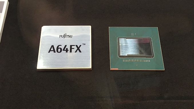
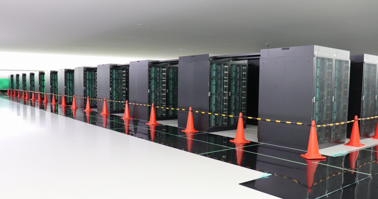
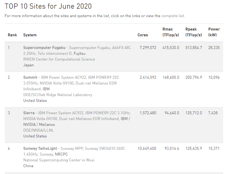
High performance computing is now at a point in its existence where to be the number one, you need very powerful, very efficient hardware, lots of it, and lots of capability to deploy it. Deploying a single rack of servers to total a couple of thousand cores isn’t going to cut it. The former #1 supercomputer, Summit, is built from 22-core IBM Power9 CPUs paired with NVIDIA GV100 accelerators, totaling 2.4 million cores and consuming 10 MegaWatts of power. The new Fugaku supercomputer, built at Riken in partnership with Fujitsu, takes the top spot on the June 2020 #1 list, with 7.3 million cores and consuming 28 MegaWatts of power.
The new Fugaku supercomputer is bigger than Summit in practically every way. It has 3.05x cores, it has 2.8x the score in the official LINPACK tests, and consumes 2.8x the power. It also marks the first time that an Arm based system sits at number one on the top 500 list.
Due to the onset of the Coronavirus pandemic, Riken accelerated the deployment of Fugaku in recent months. On May 13th, Riken announced that more than 400 racks, each featuring multiple 48-core A64FX cards per server, were deployed. This was a process that had started back in December, but they were so keen on getting the supercomputer up and running to assist with the R&D as soon as possible – the server racks didn’t have their official front panels when they started working. There are still additional resources to add, with full operation scheduled to begin in Riken’s Fiscal 2021, suggesting that Fugaku’s compute values on the top 100 list are set to rise even higher.
Alongside being #1 in the TOP500, Fugaku enters the Green500 List at #9, just behind Summit, and below the Fugaku Prototype installation which sits at #4.

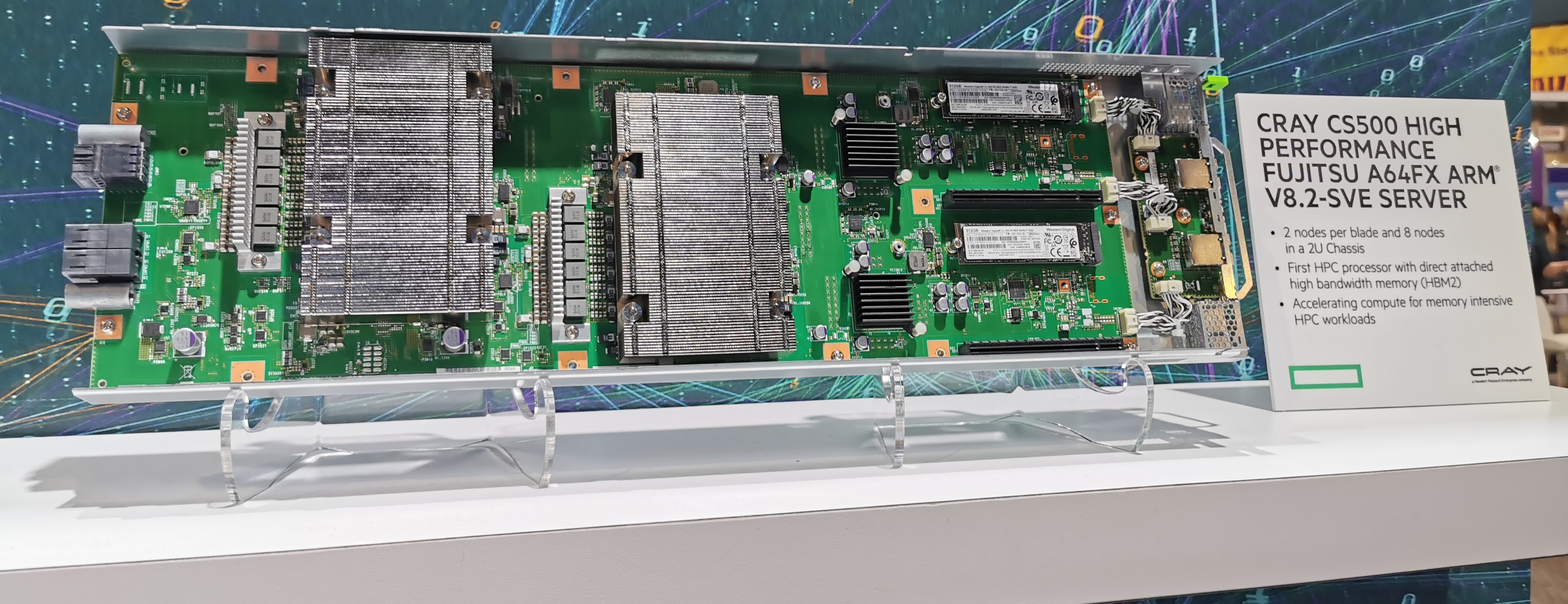
At the heart of Fugaku is the A64FX, a custom Arm v8-A CPU-based chip optimised for compute. The total configuration uses 158,976 of these 48+4-core cards, running at 2.2 GHz peak performance (48 cores for compute, 4 for assistance). This allows for some substantial Rpeak numbers, such as 537 PetaFLOPs of FP64, the usual TOP500 metric. But A64FX also supports quantized models with lower precision, which is where we get into some fun numbers for Fugaku:
- FP64: 0.54 ExaFLOPs
- FP32: 1.07 ExaOPs
- FP16: 2.15 ExaOPs
- INT8: 4.30 ExaOPs
Due to the design of the A64FX, it also allows for a total memory bandwith of 163 PetaBytes per second.
To date, the A64FX compute card is the only implementation of Arm’s v8.2-A Scalable Vector Extensions (SVE). The goal of SVE is to allow Arm’s customers to build hardware with vector units ranging from 128-bit to 2048-bit, such that any software that is built to run on SVE will automatically scale regardless of the SVE execution unit size. A64FX uses two 512-bit wide pipes per core, with 48 compute cores per chip, and also adds in four 8 GiB HBM2 links per chip in order to feed the units for 1 TiB/s of total bandwidth into the chip.
As listed above, the unit supports INT8 through FP64, and the chip has an on-board custom Tofu interconnect, supporting up to 560 Gbps of interconnect to other A64FX modules. The chip is built on TSMC’s N7 process, and comes in at 8.79 billion transistors. 90% execution efficiency is claimed for DGEMM type workloads, and additional mechanisms such as combined gather and unaligned SIMD loading are used to help keep throughput high. There is also additional tuning that can be done at the power level for optimization, and extensive internal RAS (over 128k error checkers in silicon) to ensure accuracy.

Details on the A64FX chip were disclosed at Hot Chips in 2018, and we saw wafers and chips at Supercomputing in 2019. This chip is expected to be the first in a series of chips from Fujitsu along a similar HPC theme.

Work done on Fugaku to date includes simulations about Japan’s COVID-19 track and tracing app. According to Professor Satoshi Matsuoka, predictions calculated by Fugaku suggested a 60% distribution on the app development in order to be successful. Droplet simulations have also been performed on virus activity. Deployment of A64FX is set to go beyond Riken, with Sandia Labs to also have an A64FX system based in the US.
Source: TOP500
Related Reading
- A Success on Arm for HPC: We Found a Fujitsu A64FX Wafer
- Hot Chips 2018: Fujitsu's A64FX Arm Core Live Blog


46 Comments
View All Comments
yetanotherhuman - Tuesday, July 7, 2020 - link
Hm, if memory serves, the BBC Micro used a MOS 6502 like the NESname99 - Monday, June 22, 2020 - link
You don't think it's sigificant that you can hit the same (Linpack) performance/watt as a GPU, but on a system that's a much more "traditional" architecture (ie easier to port to, easier to match to a variety of different algorithms)?Which gets at the second point: Linpack, ie dense linear algebra, is well known to be a terrible metric of this type of machine -- if what you want is dense linear algebra, you can do far better on dedicated hardware (that's why everyone is adding TPU's to their designs...).
Much more interesting is the performance on something that's not quite so trivial. There Fujitsu gets closer to 4.6x the IBM/nVidia result. So roughly they're 30% more efficient than IBM/nV for more "generic" code.
Robin Whittle - Tuesday, June 23, 2020 - link
The most important aspect of this system is its HBM (High Bandwidth Memory) - broad, very fast, connections to fast memory chips. These need to be physically close to the CPU chip. There are no DIMMs in this system.With a quick search I didn't find any concrete details on the HBM, but this page has a picture of two HBM chip per 12 (or 13) cores: https://www.reddit.com/r/Amd/comments/9vyd1h/intel... .
Main memory bandwidth has been the biggest bottleneck for most computing for decades, other that which can be done with GPUs.
Does this device have a single memory space, or do the four quadrants of 12 (13) cores each have their own space. If the former, then there will be a big latency and bandwidth restriction accessing data in the HBM chips of the three other quadrants. If the former, then the total RAM available to programs is set by the size of the two HBM chips.
Can anyone point to more details on the HBM used in Fugaku?
anonym - Monday, June 29, 2020 - link
Four CMG(Core Memory Group) connected to 8GiB HBM chip each.https://www.hpci-office.jp/invite2/documents2/ws_m...
BurntMyBacon - Wednesday, June 24, 2020 - link
Yeah, Single Board Computers are not exactly common place in your typical commercial space or even much of the professional industry as far as I can tell. I've only actually come across them in the super computing space, avionics, and a handful of other embedded systems scenarios. I might have made the same mistake.Santoval - Sunday, June 28, 2020 - link
So ExaFLOP computing was just achieved - well, for single precision (FP32) computing anyway. And only for peak performance, not max sustained.