Next-Gen NVIDIA Teslas Due This Summer; To Be Used In Big Red 200 Supercomputer
by Ryan Smith on January 31, 2020 5:00 PM EST- Posted in
- GPUs
- Tesla
- NVIDIA
- Machine Learning
- Supercomputers
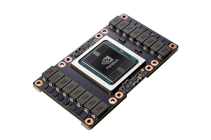
Thanks to Indiana University and The Next Platform, we have a hint of what’s to come with NVIDIA’s future GPU plans, with strong signs that NVIDIA will have a new Tesla accelerator (and underlying GPU) ready for use by this summer.
In an article outlining the installation of Indiana University's Big Red 200 supercomputer – which also happens to be the first Cray Shasta supercomputer to be installed – The Next Platform reports that Indiana University has opted to split up the deployment of the supercomputer in to two phases. In particular, the supercomputer was meant to be delivered with Tesla V100s; however the university has instead opted to hold off on delivery of their accelerators so that they can instead have NVIDIA’s next-generation accelerators, which would make them among the first institutions to get the new accelerators.
The revelation is notable as NVIDIA has yet to announce any new Tesla accelerators or matching GPUs. The company’s current Tesla V100s, based on the GV100 GPU, were first announced back at GTC 2017, so NVIDIA’s compute accelerators are due for a major refresh. However it’s a bit surprising to see anyone other than NVIDIA reveal any details about the new parts, given how buttoned-down the company normally is about such details.
At any rate, according to Indiana University the group expects to have their new accelerators installed by later this summer, with Big Red 200 running in CPU-only mode for now. The Next Platform article goes on to state that the newer accelerators will deliver “70 percent to 75 percent more performance” than NVIDIA’s current V100 accelerators, which assuming it’s accurate, would make for a hefty generational upgrade in performance. Though as always, with multiple modes of compute involved – everything from straight FP32 vector math to tensor operations to low precision operations – the devil is in the details on where those performance gains would most be realized.
In the meantime, NVIDIA’s next GTC event is scheduled for mid-March. So if NVIDIA is planning to launch a new Tesla, then I would certainly expect to see it there.
Source: The Next Platform


38 Comments
View All Comments
MASSAMKULABOX - Sunday, February 2, 2020 - link
IF tensor cores were just grouped shaders , then surely the performance of those could be put to use in non-RT games , that doesnt seem to be evident in all the benchmarks . Or even firestrike/Furmark . I mean you could be right .. I thought RT logic was unused in non RT games.. Maybe I'm hopelessly confused with RT tensor Ai acceleration etc etc etcedzieba - Sunday, February 2, 2020 - link
"Just to be clear, Tensor Cores don't exist as separate logic. They are just groups of 8 shaders being used together to carry out operations more efficiently than if they were doing the same calculations as individual instructions. "This is incorrect. Not only can Tensor cores and CUDA cores operate simultaneously, there are not a sufficient number of CUDA cores to perform the number of simultaneous operations that the Tensor cores perform. 64x operations per Tensor core to perform a single 4x4 FMA operation, not 8x operations, because that's not how matrix math works. This has been proven by independant benchmarking (e.g. Citadels microarchitecture analysis: https://arxiv.org/pdf/1804.06826.pdf found Tensor TFLOPS to match the published values for Tensor cores, a peak impossible to achieve with the number of CUDA cores on the die).
The reason a Tensor core can do so many individual operations without taking up too much diea rea is because they are fixed-function: a Tensor core will do an FMA operation on predetermined size input and output matrices, and that's all they'll do. If you feed them a scaler (packed into a matrix) then most of the core will be doing nothing. a CUDA core on the other hand is a multipurpose engine, it can perform a huge variety of operations at the cost of increased die area per core. You could take 64 CUDA cores and perform the same 4x4 FMA operation that a Tensor core performs, but it would take both longer (due to the need to corral 64 cores worth of memory operations) and use up a vastly larger die area. You CANNOT take a Tensor core and split it into 64 individually addressable units however.
Note that at a hardware level, a 'Tensor core' sits within a sub-core within an SM, alongside the general purpose math engines for FP and INT operations. For Volta, the Tensor core and one of the GP math cores could operate concurrently. For Turing, the FP and INT cores can also operate concurrently alongside the Tensor core.
Yojimbo - Sunday, February 2, 2020 - link
Let's look at the RTX 2060. It has 1920 32-bit stream processors and 240 tensor cores. That enables 3840 FP16 FMA operations per clock. According to NVIDIA's blog on tesnor cores "Each Tensor Core performs 64 floating point FMA mixed-precision operations per clock". 240x16 = 3840. A coincidence? Maybe, but there are certainly a sufficient number of CUDA cores to handle the simultaneous operations.The caveat I see here is that the Tensor cores include a 32 bit accumulate. Perhaps each FP32 ALU that is used to initially hold two FP16 inputs can successfully hold the FP32 result with the correct circuitry. There then needs to be an FP32 accumulator to add all the correct products together. I really don't know anything about electronic engineering. I guess they can cascade the results somehow to use the accumulation circuitry of the cores to take their own product results and add them to a cascading sum of other cores' product results. The first core in the line would add the already stored result from the neural network with the first product, then the second in line would take that combined value and add it to its own product result, etc. This all needs to be done in one clock cycle. It would demand some sort of sub-cycle timing so that all it can be performance. But maybe the core clock of the GPU is in reference to the scheduler and warp operations, and the internal core operations can have more finely grained timings. (??)
SaberKOG91 - Monday, February 3, 2020 - link
Yeah, I don't know where they are getting their math from either. Each tensor core is able to do 64 FMA ops per cycle with FP16 inputs. This works out to exactly 8 FMA operations per CUDA core, with a row-column dot-product requiring 4 multiplies and 3 additions, plus 1 more addition for the final accumulate (4xFMA). This allows 8 shaders to compute the full 4x4 tensor FMA in 1 cycle. It also holds that the FP16 Tensor TFLOPS are almost exactly 8x the FP32 TFLOPs, but only 4x the FP16 TFLOPS. With some clever use of data locality in the hardware, I can absolutely see them getting these kinds of results.Yojimbo - Sunday, February 2, 2020 - link
I also scanned the introduction (summary and chapter 1), conclusion, and tensor core sections of the paper you posted and didn't see them make your claimed conclusions: 1) tensor cores and CUDA cores can operate simultaneously, or 2) there are not sufficient number of CUDA cores to perform the simultaneous operations, including that they showed a peak impossible to achieve with the number of CUDA cores on the die. What they do show is that 16-bit-result tensor core operations show a capability of only reaching 90% of its peak theoretical result and that 32-bit-result only seems to achieve about 70%. That means that the circuitry is not able to achieve its peak theoretical result like clockwork, unlike the basic FMA operations as shown in the two graphs (the ones with red or blue lines) below the tensor core graph. That is interesting because it shows that the tensor core operation is some complex operation that doesn't always go through as intended. I'd argue that if NVIDIA created a special block of execution units to run the operation that would be less likely to happen. Incidentally, I have the vague notion reading that the Turing tensor cores achieve closer to their peak theoretical performance when performing their intended operation. Additionally, the fact that the 16-bit-result gets closer to its peak performance than the 32-bit-result is also interesting. It suggests that the 32-bit-result operation is trying to squeeze even more out of re-purposed circuitry than the 16-bit-result, which fits with the complications of 32 bit accumulation I proposed in my previous post. And again, if NVIDIA had free reign to purpose-build a new fixed-function block it would be expected that they would achieve full peak throughput under ideal conditions for its intended operation (the matrix multiply and accumulate). It really suggests a clever re-purposing to me.In any case, if you can be more specific as to where and how in the paper they prove your conclusions it would be helpful, because I was unable to see it on my own.
trinibwoy - Tuesday, February 4, 2020 - link
Peak fp16 tensor flops are 4x the peak regular fp16 flops on Turing.It is not possible to achieve the tensor peak using regular CUDA cores. Therefore the tensor cores must be separate hardware.
SaberKOG91 - Thursday, February 6, 2020 - link
Not necessarily. It just means that the math being done in the hardware uses some trick to perform multiple equivalent operations in a single cycle. This isn't really any different than an FMA instruction resulting in two operations per cycle. It's far more likely that each CUDA core has a little bit of extra area allocated to additional optimized instructions which, because of datapath limitations, aren't usable in normal FP16 operation, but can be used in optimal circumstances to perform 8 multiplies and 8 additions in a single cycle. This is easily explained by pipelining. Turing takes 4 cycles to complete a single warp. Each CUDA core can do 1 FP32 FMA in this time, but with pipelining the average cost goes down to 1 cycle. If Nvidia were able to cleverly use each pipeline stage to do an FP16 FMA, each CUDA core could execute 16 FMA operations per cycle and a total of 64 FMA operations by the end of the pipeline. This would mean an average of 64 FMA operations per cycle, which is exactly as advertised. The same throughput is not achievable with normal FP16 ops because the bandwidth requirements are too high. This technique relies on operands moving through the pipeline and being reused each cycle.p1esk - Friday, January 31, 2020 - link
A few thoughts:1. Nvidia needs to make a specialized DL chip (get rid of FP64 cores) to compete with TPUs
2. We are talking about Tesla cards, which don't have output ports, so talking about HDMI 2.1 or DP 2.0 does not make sense.
3. PCIe 4.0 is good but it's not good enough. What we need is an ability to link more than 2 cards with NVlink using bridges.
4. Put more memory on these cards. TPUs let you use insane amount of memory to train large models (like GPT-2). Right now I'm planning to build quad Quadro 8000 (instead of Titan RTX, because I need the memory).
Yojimbo - Saturday, February 1, 2020 - link
NVIDIA have specialized DL chips. They don't feel they need to commercialize one at the moment. Bill Dally, NVIDIA's chief scientist, claims they can come out with one or add it to one of their products whenever they want to.Santoval - Saturday, February 1, 2020 - link
Internal testing of unreleased products and empty claims of the "We can do xx as well!" kind are irrelevant at best, meaningless at worst. All companies have R&D labs, the point is what they choose to do with that research, what to release. As long as Item X remains in the R&D wing of a company, it effectively does not exist outside of it.