Micron’s Fab 10 Expansion Completed: 96-Layer 3D NAND Production Starts in 2019
by Anton Shilov on August 16, 2019 4:30 PM EST
Micron this week hosted a grand opening ceremony of its Fab 10 Expansion in Singapore. The new cleanroom is not expected to increase the company’s production capacity in terms of wafer starts per month, but will enable Micron to continue adopting more advanced 3D NAND process technologies with a higher number of layers and bit density.
The new Singapore Fab 10 Expansion is an integral part of Micron’s Fab 10 complex that was previously comprised of Fab 10N and Fab 10X. Officially, it's known that the new 3D NAND production facility is built on a 165,000 m2 land plot, however Micron is not disclosing much else about the usable cleanroom space or other features of the expansion.
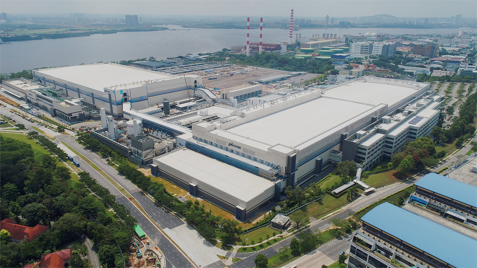
Micron is now installing equipment and expects to start production of 96-layer 3D NAND at the new Fab 10 Expansion sometime in the second half of this calendar year (i.e. in the next 4.5 months). Meanwhile, the company stresses that it will align its spending on production tools with 3D NAND demand and trends. Furthermore, even when fully equipped, the facility is not expected to add any new wafer capacity, but rather will be used to house more advanced process equipment necessary for greater numbers of 3D NAND layers.
As the number of 3D NAND layers increases, each wafer has to spend more time inside chemical vapor deposition (CVD) machines, meaning it takes longer to etch them. Adding more time still, various extravagant production techniques like string stacking lengthen manufacturing require even more steps. In order to keep the number of wafers processed consistent as the number of 3D NAND layers grows, flash memory producers have to add extra CVD and etching machines to cleanrooms, which requires extra space. As a result, while bigger fabs may not increase the number of wafer starts per month, they do enable growth in terms of produced NAND flash bits.

Along with the new manufacturing plant, Micron is also expanding its R&D operations in Singapore. Micron’s NAND Center of Excellence will among other things perform technology development and product engineering. Considering how close these functions will be to the actual production facility, the company certainly hopes to improve its yields and productivity at Fab 10.
Related Reading:
- Micron to Expand Its Fab 6 in Virginia, Build New R&D Center
- Micron Starts Construction of Its Third NAND Fab in Singapore
- Intel and Micron To Dissolve 3D XPoint Partnership After 2019
- Intel And Micron To Discontinue Flash Memory Partnership
- Micron Hires New CEO: Sanjay Mehrotra, SanDisk Co-Founder And Former CEO
Sources: Micron, The Strait Times


21 Comments
View All Comments
eek2121 - Monday, August 19, 2019 - link
It'll get there eventually. That's why I question the wisdom of continuing hard drive production at all. I've had tons of problems with hard drives, but no problems with SSDs dating all the way back to the first gen 120 gb drives.The one thing that is going to hinder lower prices is a lower adoption rate due to decreased failures. For instance, Seagate is widely known as a budget brand for hard drives. Their drives are often among the cheapest around, but they can have high failure rates depending on the drive/capacity. At one company, we added a 48 bay NAS with 120gb SSDs in RAID, and there hasn't been a single drive failure yet. Compare that to the previous NAS that had a bunch of spinning drives and you had a drive fail every 6-18 months. The NAS in question has been in use for MANY years now and it wasn't cheap to put together, but the performance impact was worth it. The 10 Gbit link to the graphics editors from the rack means that they are able to pull down graphics and video quite fast.
With that kind of reliability, the floor for SSDs will always be higher than HDDs. There isn't any getting around it. Even if you warrantied your defective hard drives, you still had to buy a new one or keep a few spare on hand just so you could get that RAID rebuilt ASAP. With hard drives, most companies wouldn't bother with the RMA due to the time it takes to RMA the drive, send it in, track the progress, and get it back because it often costed more than simply purchasing a new drive.
Come to think of it, I don't recall a single company I ever worked at that RMAed a hard drive. I have personally, but never at a company. We would just pop in a new one and send the defective one to the shredder.
deil - Monday, August 19, 2019 - link
Well 1TB of ssd != 1TB of FAST ssd. I expect 5GB/s in that drive for 80$ and current one will not reach full sata speeds...deil - Monday, August 19, 2019 - link
well problem grows faster than linear so 512 might end up with problems we dont even dream about now. Overheat of "middle layers" or something that is bizarre right now, with 1024 stacks will happen. I think we will stop on ~384'ish per stack.QUOTING:
"What is important is that Samsung plans to use its 136-layer architecture with speed-optimized circuit design to build V-NAND devices with over 300 layers by mounting three of the current stacks on top of each other (thus tripling a chip’s capacity)."
So it will end up as ~3x384'ish per die ~700 Gb so 3 chips for 256 GB drive...
as current best 256 Gb chips cost ~60$ in final product, we can expect 1TB in ~70-80$ brackets in ~1.5 years.
eek2121 - Monday, August 19, 2019 - link
It doesn't 'drive down cost'. If a 256 gb SSD costed $50 to make in say, 2016 and now the 512 gb costs $50 to make, that isn't 'lost revenue'. Margins aren't driven down by capacity increases, but instead they are driven down by competitive pressure.ksec - Saturday, August 17, 2019 - link
I wish Anandtech comment has a tag system so I could tag those who call people idiot, naive, stupid ( to quote their words) for saying NAND and DRAM are price fixing Cartel and market manipulation.The amount of engineering required in modern day NAND and DRAM, and cost of R&D and Fab Expansion is quite insane.
melgross - Monday, August 19, 2019 - link
Well, while not all of this is price fixing, Samsung, for example, has been convicted of NAND price fixing already. Same thing for LCD panels and other things. In fact, several years ago, Apple was going to open a memory plant with Samsung, but after Samsung’s conviction, which resulted in another several hundred million dollar fine, decided not to.quadibloc - Saturday, August 17, 2019 - link
Actually, it was before we had EUV that we had to do really crazy things to make chips that had features smaller than the wavelength of the light used to make them - stuff like quadruple patterning. Making the chips in a vacuum, using shallow reflection off hyperbolic mirrors to focus the EUV light, by comparison, those aren't crazy things, that's just what you have to do to use that kind of light (if you can call it that instead of soft X-rays).FreckledTrout - Sunday, August 18, 2019 - link
So you don't think using a laser that is the size of 5 refrigerators to generate a high intensity laser beam that is strobed low/high over and over to hit tin droplets being fired at 100mph in a vacuum to just create the light is not complex? The low strobe hits the tin to spread the droplet flat then the high one obliterates it to create the EUV. This sounds a tad complex to me. /smhhttps://www.youtube.com/watch?v=5yTARacBxHI
ironwing - Sunday, August 18, 2019 - link
Doesn't each new layer require additional vertical vias passing through the layers below? I'm imagining this as requiring a dedicated elevator shaft for each layer. Eventually the horizontal footprints of the elevator shafts passing through the lower layers cancels out the extra space gained by adding the next layer.sor - Friday, August 16, 2019 - link
Awesome news. I don’t work for Micron any more but I went to Singapore and bootstrapped the two dozen or so racks of infrastructure to run the initial Fab 10 green field build, in 2007 or so. I always enjoy hearing about where they are now.