TSMC Announces Performance-Enhanced 7nm & 5nm Process Technologies
by Anton Shilov on July 30, 2019 6:00 PM EST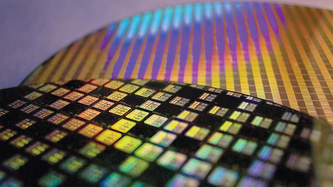
TSMC has quietly introduced a performance-enhanced version of its 7 nm DUV (N7) and 5 nm EUV (N5) manufacturing process. The company’s N7P and N5P technologies are designed for customers that need to make then 7 nm designs run faster, or consume slightly lower amount of power.
TSMC’s N7P uses the same design rules as the company’s N7, but features front-end-of-line (FEOL) and middle-end-of-line (MOL) optimizations that enable to either boost performance by 7% at the same power, or lower power consumption by 10% at the same clocks. The process technology is already available to TSMC customers, the contract maker of chips revealed at the 2019 VLSI Symposium in Japan, yet the company does not seem to advertise it broadly.
N7P uses proven deep ultraviolet (DUV) lithography and does not offer any transistor density improvements over N7. Those TSMC clients that need a ~ 18~20% higher transistor density are expected to use N7+ and N6 process technologies that use extreme ultraviolet (EUV) lithography for several layers.
While both N7 and N6 will be ‘long’ nodes that will be used for years to come, TSMC’s next major node with substantial density, power, and performance improvements is N5 (5 nm). The latter will also be offered in a performance-enhanced version called N5P. This technology will also feature FEOL and MOL optimizations in order to make the chips run 7% faster at the same power, or reduce consumption by 15% at the same clocks.
Related Reading:
- TSMC: Most 7nm Clients Will Transition to 6nm
- TSMC Reveals 6 nm Process Technology: 7 nm with Higher Transistor Density
- TSMC’s 5nm EUV Making Progress: PDK, DRM, EDA Tools, 3rd Party IP Ready
- TSMC: 7nm Now Biggest Share of Revenue
- TSMC: First 7nm EUV Chips Taped Out, 5nm Risk Production in Q2 2019
- TSMC Details 5 nm Process Tech: Aggressive Scaling, But Thin Power and Performance Gains
- Intel Details Manufacturing through 2023: 7nm, 7+, 7++, with Next Gen Packaging
Source: WikiChip.Org


36 Comments
View All Comments
Rudde - Wednesday, July 31, 2019 - link
Wider cores, more cache and better predictors all help single core performance. E.g. Ice lake has similiar single core performance to Whiskey lake, even though Ice lake runs 1GHz slower. Gaming has seen used threads climb towards 16 threads, where as a few years ago 8 threads was the maximum.There is a shift toward accelerators doing the heavy work and cpus being used for shifting data and light processing.
name99 - Wednesday, July 31, 2019 - link
Try looking outside the x86 bubble...Plenty of people ARE finding remarkably interesting ways to keep using more transistors. But those people don't work for INTC or AMD.
ET - Wednesday, July 31, 2019 - link
I wonder if AMD will use it for the next gen APU.ToTTenTranz - Wednesday, July 31, 2019 - link
I'm struggling with the suggestion that N6 will be a "long node", considering it's coming out just months before N5, and N7+ with better performance is reportedly being used for volume production already.I get that we might see slight refreshes of Navi 10 and Zen 2 chiplets, but I doubt very high-volume mobile SoC vendors like Qualcomm and Apple will choose to reuse designs for N6 instead of making something from the ground up for N7+. And for 2021 updates they'll most probably use N5.
Rudde - Wednesday, July 31, 2019 - link
TSMC is trying to get 28nm customers over to N7. Those customers can move to N6 without having to redesign. TSMC expects those customers to stay at N6 for a long time.Gondalf - Wednesday, July 31, 2019 - link
Intel advetrise Ice Lake like plain 10nm, from the official process roadmap 10nm+ will be available only in 2020 with the Willow Cove core. If old data are valid at that point 14nm and 10nm will have the same drive current.This is consistent with some voices about a Sunny Cove/Willow Cove S for desktop in 2H/2020.
But i think the situation is fliud, the only certain thing is about a "silicon back" of Tiger Lake (Willow Cove +Xe) for Laptops.
In 2021 there will be 10nm ++ and first edition of 7(5)nm process.