TSMC Announces Performance-Enhanced 7nm & 5nm Process Technologies
by Anton Shilov on July 30, 2019 6:00 PM EST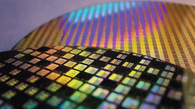
TSMC has quietly introduced a performance-enhanced version of its 7 nm DUV (N7) and 5 nm EUV (N5) manufacturing process. The company’s N7P and N5P technologies are designed for customers that need to make then 7 nm designs run faster, or consume slightly lower amount of power.
TSMC’s N7P uses the same design rules as the company’s N7, but features front-end-of-line (FEOL) and middle-end-of-line (MOL) optimizations that enable to either boost performance by 7% at the same power, or lower power consumption by 10% at the same clocks. The process technology is already available to TSMC customers, the contract maker of chips revealed at the 2019 VLSI Symposium in Japan, yet the company does not seem to advertise it broadly.
N7P uses proven deep ultraviolet (DUV) lithography and does not offer any transistor density improvements over N7. Those TSMC clients that need a ~ 18~20% higher transistor density are expected to use N7+ and N6 process technologies that use extreme ultraviolet (EUV) lithography for several layers.
While both N7 and N6 will be ‘long’ nodes that will be used for years to come, TSMC’s next major node with substantial density, power, and performance improvements is N5 (5 nm). The latter will also be offered in a performance-enhanced version called N5P. This technology will also feature FEOL and MOL optimizations in order to make the chips run 7% faster at the same power, or reduce consumption by 15% at the same clocks.
Related Reading:
- TSMC: Most 7nm Clients Will Transition to 6nm
- TSMC Reveals 6 nm Process Technology: 7 nm with Higher Transistor Density
- TSMC’s 5nm EUV Making Progress: PDK, DRM, EDA Tools, 3rd Party IP Ready
- TSMC: 7nm Now Biggest Share of Revenue
- TSMC: First 7nm EUV Chips Taped Out, 5nm Risk Production in Q2 2019
- TSMC Details 5 nm Process Tech: Aggressive Scaling, But Thin Power and Performance Gains
- Intel Details Manufacturing through 2023: 7nm, 7+, 7++, with Next Gen Packaging
Source: WikiChip.Org


36 Comments
View All Comments
FreckledTrout - Tuesday, July 30, 2019 - link
TSMC is being somewhat quiet about it but it's very likely the 5nm node will be some variant of GAA using nanosheets.name99 - Wednesday, July 31, 2019 - link
TSMC 5nm is already locked in, and it is FinFET, not GAA.https://www.tsmc.com/english/dedicatedFoundry/tech...
Threska - Saturday, August 3, 2019 - link
https://spectrum.ieee.org/semiconductors/devices/t...Still rather unproven.
Santoval - Tuesday, July 30, 2019 - link
GAA-FETs will be introduced at the 3/4nm node of the foundries, and possibly Intel's 7nm node.LordSojar - Wednesday, July 31, 2019 - link
Right. Exactly Santoval. It's at this juncture we may really begin to see some decent speed increases, and that's a big maybe. That was why I made the point earlier about increasing efficiency, branching out architecture designs, and making each processor do more per cycle. GAA may allow for 5-7GHz if it's done in the manner they're describing (and not some pseudo-tech/science marketing jargon, which is all that these transistor size measurements have become at this point)Santoval - Tuesday, July 30, 2019 - link
"Making each core do more" in what way exactly? A +7% performance at the same TDP suggests +7% higher clocks at the same TDP, assuming an identical μarch and CPU design. We are talking purely about the performance of the *node* here, so the μarch and the design of the CPU is irrelevant."more efficient at doing the same per cycle is better." Yes, that's swell, but that's just an alternative to the mentioned +7% higher performance of the article. It's an "either or" situation, as always : Either you retain the same TDP and extract 7% higher performance (via 7% higher clocks assuming an identical design) or you retain the same performance and lower your TDP budget by 10% at 7nm and 15% at 5nm.
7% higher clocks of the Ryzen 3000 series means 300 MHz higher base & boost clocks on average. Yes, it is harder to raise clocks with each smaller node due to the reasons you mentioned. However the Ryzen 3000 series was released on TSMC's original high performance 7nm node iteration. There is nothing to suggest that the clocks of the Ryzen 3000 series are the max clocks TSMC can reach at 7nm.
Further optimizing their 7nm node (without increasing its density and thus using smaller features at all, which is important) will allow them to reach 7% faster clocks at the same TDP (at least according to them, I am skeptical until I see products) *or* reducing the node's TDP further, which is just as important. The clocks of their 7nm+ and 6nm node will obviously be lower, due to the higher density of these nodes.
There is obviously a finite limit of ~5GHz single core clocks at a TDP of up to ~100W, and that cannot be normally exceeded due to the collapse of Dennard scaling and the slowing down of Koomey's law. The.. abnormal exception is Intel, since according to leaks their top end Comet Lake CPU will reach a single core boost clock of 5.2 GHz. That's because they have been optimizing their 14nm node since ... 2014, and bizarrely in 2020 they will still be releasing 14nm node based CPUs (after Comet Lake comes Rocket Lake) due to the continuing severe issues of their 10nm+ node.
ZolaIII - Wednesday, July 31, 2019 - link
Actually design of cores and ISA have a lot of to do with performance per W & so does the design choice not to persuit the insane clocks. Uper sustainable leaking limit for FinFET is 1.6~1.7 GHz, the final limit should be 2~2.2 GHz which we still see on power optimised many core systems (server chips). Choosing the HD libs instead HP ones when designing power optimised chip will hurt only 100~200 MHz on performance target while it can cut the size/power consumption by up to 50% which we see in mobile (phone) SoC's. The simple OoO designed core like A73 two instructions wide is still about 3~3.5x the size of an in order A55 while performance benefit is about 1.73~1.8x, as you go wider things only get worse regarding those metrics. Scalable ISA (beyond the 64 bit) regarding front end is a key for future performance benefits, especially for SIMD's & DSP's. Simplicity of ISA is crucial for replicating 64 bit general processing blocks (both integer and FP) & tieing them together to work as one, as waiting for instruction execution is also minimised. It's also easyer in such a case to make a simple predictor to go with micro switch. Leading ISA regarding all mentioned is of course RISC V (simplicity, 128 bit finalised & 256 bit on paper) while no one still didn't consider this approach seriously which I hope will change along with unified SIMD approach for which RISC V also left open doors (considering balanced design).Gondalf - Wednesday, July 31, 2019 - link
Very unlikely AMD will adopt this new process. It need of a new masks set and it is pretty expensive. Reportedly they want 7nm+ instead.Moreover IMO these clock speed increases are likely on low power phone socs, a little tricky on high power SLUs were the huge 7nm leakage destroy any power saving features implemented on processes.
Nearly nothing for too much money in manufacturing
RSAUser - Thursday, August 1, 2019 - link
Not all numbers are equal, Intel 14nm++ 5GHz is probably about 4.4-4.5GHz Ryzen 3000 7nm performance, if not a little lower since it's ~15% IPC gain over Intel's.FreckledTrout - Tuesday, July 30, 2019 - link
If we are taking about AMD moving to TSMC's N7+ for Ryzen 4000 then I don't think boosting to 5Ghz is out of the question in fact it's expected.