Phison’s Next-Gen eSSD Controllers to Support Everspin’s STT-MRAM Caching
by Anton Shilov on July 25, 2019 10:00 AM ESTPhison and Everspin on Wednesday said that the former's upcoming controllers for enterprise-grade SSDs would natively support the latter’s spin torque transfer MRAM (STT-MRAM) that will be used as a write buffer to enable a more effective I/O management. The new technology will allow makers of SSDs to improve I/O performance of their drives and enable power loss protection without usage of supercapacitors.
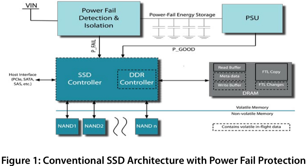
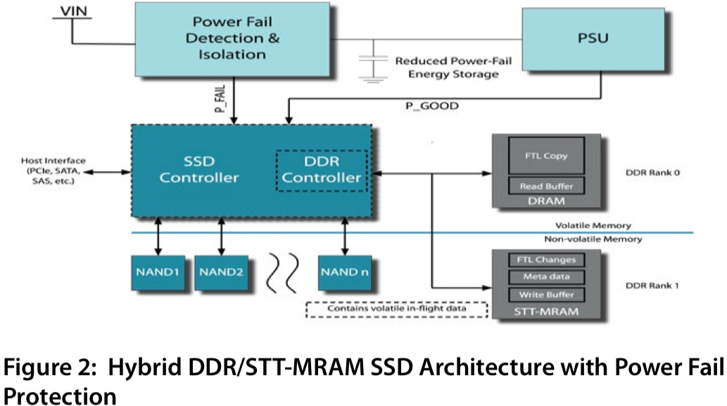
The upcoming eSSD controllers from Phison will support Everspin’s 1 Gb STT-MRAM memory “to increase the reliability and performance” of next-gen server-grade SSDs. In particular, the companies say that STT-MRAM chips will enable SSD makers to more effectively manage I/O streams, which will enable for better latency determinism and therefore improve QoS. Besides, since STT-MRAM is nonvolatile, drives that will use it instead of traditional DRAM buffers will not need a sophisticated power loss protection enabled by supercapacitors, which will simplify their physical architecture and will enable to increase their capacity by adding more 3D NAND packages.
As far as performance of STT-MRAM-enabled SSDs is concerned, the buffer and appropriate software can lower overall latency and increase random performance of drives significantly versus typical SSDs. It is of course too early to say anything about SSDs based on next-generation controllers from Phison, but the partnership between the two companies promises to bring significant performance enhancements to upcoming storage subsystems.
Phison’s SSD partners won't the first to use STT-MRAM as write cache buffers for 3D NAND-based SSDs. Both IBM and Seagate already offer appropriate drives commercially today. Meanwhile, native support of STT-MRAM by SSD controllers will make it considerably cheaper and easier for drive makers to build such products.
Phison and Everspin will discuss use cases of STT-MRAM in enterprise storage applications at Flash Memory Summit in early August.
Related Reading:
- Everspin Begins Production of 1Gb STT-MRAM
- IBM And Everspin Announce 19TB NVMe SSD With MRAM Write Cache
- Seagate Demos New SSD Features And Prototypes At FMS
- Everspin Announces New MRAM Products And Partnerships
Source: Phison


20 Comments
View All Comments
Diogene7 - Thursday, July 25, 2019 - link
I am really looking forward for MRAM (STT-MRAM, or even better SOT-MRAM) to come to consumer grade products : I believe it has the potential to be a key enabler of significant improvement in reducing latency to access code / data, and therefore significantly improve the end user experience (a bit like SSD brought much improvement compare to mechanical HDD)name99 - Thursday, July 25, 2019 - link
Is write protection the ONLY thing they are using the MRAM for?I'd have thought there'd be opportunity to use the MRAM to hold the FTL. That's mostly a read use-case, so the fact that MRAM has slower writes than DRAM (but, supposedly equal to rather faster reads) would be fine. And then you have the opportunity for cost saving (or at least cost parity) by dropping the DRAM...
The real problem, I guess, is that as outsiders we have no idea what the specs are for current ACTUALLY SHIPPING MRAM :-( (hint, hint, AnandTech...)
We know what the theoretical profile is supposed to be in terms of read vs write performance, energy usage, density, granularity, cost, etc -- but we have no idea of the gap between that end point and what Everspin is shipping right now...
IntelUser2000 - Thursday, July 25, 2019 - link
1Gbit is too small, which explains the specialized use case for the device.Most SSDs need 1GB of DRAM for 1TB of NAND.
ksec - Thursday, July 25, 2019 - link
It is not really the Size of NAND SSD Drive that determines the cache. If you have a SSD operating at 1GB/s, 128MB cache isn't nearly enough, as that would mean 1/8 of second buffer. For drive that are now approaching 3GB/s, and more in the future, I think capacitor makes more sense.hojnikb - Thursday, July 25, 2019 - link
DRAM cache is not used as a buffer, but only for FTL. As such, it generally needs 1GB of space for every 1TB of flash.Billy Tallis - Thursday, July 25, 2019 - link
Everspin's website has datasheets for the current 256Gb MRAM parts, including full timing information. It's not much of a mystery.name99 - Thursday, July 25, 2019 - link
If you can translate that state machine, with all the transitions, AND you have stats for average dwell times in each state, we’ll you’re way ahead of the rest of us. So inform poor dumb the rest of us of things like latencies (rd, write, what sort of variance do you see) and how much we might expect these to improve as memory controllers learn to optimize for the characteristics of this storage.Is there a significant read to write turn around time? So it makes sense to batch stores?
Is there an important granularity(like pages) with lower latency to the equivalent of an open page?
Are there similar trade offs as for DRAM for keeping pages open vs rapidly closing them?
Is there a hierarchy of components (ranks, banks, pages, ...) each corresponding to a different type of bottleneck, so that maximum throughout (and minimum latency?) is achieved by spreading data across all these levels (by address bit shuffling or otherwise)?
What are the performance characteristics of the wear-leveling?
Etc etc etc. None of this stuff Is NEARLY aaa obvious as you seem to think, at least not to me.
BTW, to other readers, the tech note on the Everspin web site discussing using MRAM on SSDs does, in fact, describe using MRAM to hold the FTL, thus removing the need for a DRAM; but seems to suggest that that’s a more demanding change than this first “write cache” change, so presumably gets implemented in the next gen of SSD controllers. (Maybe it also demands the next step larger of MRAM to be practical? though they don’t mention that.)
abufrejoval - Friday, July 26, 2019 - link
I think it's pretty great they are providing the information for free.Demanding that they educate you for free, is a little over the top, don't you think?
Of course you could do a little research, answer those questions yourself and then publish an article for free: That would benefit you and perhaps some others as well.
abufrejoval - Friday, July 26, 2019 - link
The main issue is economy not MRAM vs. DRAM speeds: Were talking about operating Flash on SSDs not HPC.So as long as MRAM is more expensive then DRAM, you only put data in it, that really benefits from the non-volatility. Read caches work just fine with DRAM, most parts of the FTL can be reconstructed after a power-fail, too, as long as the logs are secure. So the write buffer really is both on the critical timing path to acknowledge write completions to the host and for ensuring data consistency in case of a power failure.
Of course, MRAM also allows you to do more aggressive power management. These SSD controllers have embedded CPU cores with caches for code and data and if you design these caches in MRAM, saving the CPU state just means writing out the register file. Without MRAM you'd be stopping the clock but maintain enough power to hold CPU and cache state, because re-reading/re-constructing would require too much time (much like a power-fail recovery).
The latter case would require building the controller SoC on an MRAM enabled process, through, which sounds attractive for this use case, even if it's not part of part of this initial product, I believe.
flgt - Thursday, July 25, 2019 - link
Everspin really needs some good financial news.