TSMC: 3nm EUV Development Progress Going Well, Early Customers Engaged
by Anton Shilov on July 23, 2019 3:00 PM EST- Posted in
- Semiconductors
- EUV
- TSMC
- 3nm
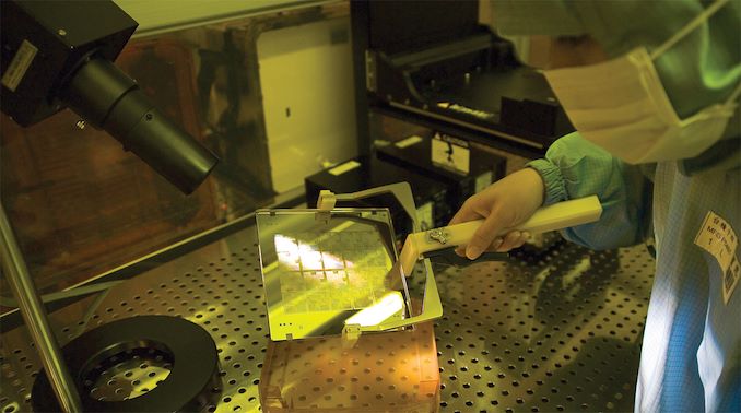
Development of new fabrication technologies never stops at leading-edge companies such as TSMC. Therefore, it is not surprising to hear the annoucement that development of TSMC’s 3nm node is well underway, something the company publicly confirmed last week. As it appears, the manufacturing technology is out of its pathfinding mode and TSMC has already started engaging with early customers.
“On N3, the technology development progress is going well, and we are already engaging with the early customers on the technology definition,” said C.C. Wei, CEO and co-chairman of TSMC, in a conference call with investors and financial analysts. “We expect our 3-nanometer technology to further extend our leadership position well into the future.”
Since its N3 technology is in its early stages of development, TSMC doesn't currently talk about the specific characteristics of the process nor its advantages over N5. TSMC said that it had evaluated all possible transistor structure options for 3nm and came out with ‘a very good solution’ for its clients. The specification is under development and the company is confident it would meet requirements of its leading partnering customer.
One of TSMC’s arch-rivals, Samsung Foundry, plans to use nanosheet-based Gate-All-Around MBCFET transistors for its own 3nm (3GAAE) process technology. Since TSMC will have to be competitive with its rival, we expect the company to also advance its 3nm node significantly in comparison to its 5nm node. In fact, TSMC confirms that N3 is a brand-new process technology, not an improvement or iteration of N5.
Meanwhile, it is safe to say that that TSMC’s 3 nm node will use both deep ultraviolet (DUV) and extreme ultraviolet (EUV) lithography equipment. Since TSMC’s N5 uses up to 14 EUV layers, it is likely that N3 will go even higher in the amount of layers employed. The world’s largest contract maker of semiconductors also seems to be quite happy with its EUV progress and considers the technology important for its future.
Related Reading:
- Samsung Announces 3nm GAA MBCFET PDK, Version 0.1
- TSMC’s 5nm EUV Making Progress: PDK, DRM, EDA Tools, 3rd Party IP Ready
- TSMC: First 7nm EUV Chips Taped Out, 5nm Risk Production in Q2 2019
- TSMC Details 5 nm Process Tech: Aggressive Scaling, But Thin Power and Performance Gains
- TSMC Starts to Build Fab 18: 5 nm, Volume Production in Early 2020
Source: TSMC


75 Comments
View All Comments
Wilco1 - Wednesday, July 24, 2019 - link
There isn't any magic quantum limit we're hitting. And ternary computing is quackery. If you said 1 in 4 hot encoding then that's a possibility, but CMOS transistors only have 2 stable states.wumpus - Thursday, July 25, 2019 - link
Last I heard (1990s? on comp.arch?), ternary had some advantages in log based computing, which could work wonders on things like GPUs and AI. Don't expect any other big benefits, as all it means is more transistors will be needed (and still leaking, and more transistor states need to change, meaning more power).Presumably any fab that can make CMOS chips out of MOSFETS could make ternary out of the same, just expect to spend a decade or two characterizing all the effects you didn't *quite* expect.
axfelix - Wednesday, July 24, 2019 - link
3nm probably won't be in mobile SoCs until closer to 2023 (maybe 2022) and will likely be the first real gain on 7nm as 5nm is looking fairly modest by comparison. And 3nm GPUs will probably be a couple years after that, 2024 at the earliest. That might be the last full shrink for a little while though.name99 - Wednesday, July 24, 2019 - link
Ending litho shrinks does not mean density stops increasing!Even with no more litho shrink, there is ample scope for growth via 3D...
(stacked N and P transistors, stacked logic, moving some metal layers below logic, ...)
wumpus - Thursday, July 25, 2019 - link
CPUs, SOCs, and GPUs have been limited by local power density for quite some time. Stacked transistors seem to work fine in NAND flash (which doesn't use so much power), but don't count on stacking logic on top of each other.There have been some [academic] improvements with moving things like initialization circuits to another level, but as local power density limits took over, I don't think there's any point in going to that well.
SaturnusDK - Wednesday, July 24, 2019 - link
It may be prudent to remember the decimals when we get to these small sizes. N3 is technically a 3.5nm density scaling target compared to N5 (or 5.2nm). N2 is 2.5nm. N1A is 1.8nm. N1B is 1.2nm.I'm not sure if any foundries are currently even doing theoretical work on sub N1B nodes.
name99 - Wednesday, July 24, 2019 - link
"3nm is looking like 2021, 3nm+ / 2nm in 2022, 2nm / 1nm in 2023, Possibly 1nm in 2024."Too optimistic. Volume 5nm is 2020, risk 3nm may be 2021, with volume 3nm 2022.
Apple ships about 200M phones a year. About 2/3 of those are leading edge, so that would be about 140M chips. iPad Pro adds something to that.
Watch we don't know --- but as of Watch 4 it's the same core, which suggests it's also fabricated on leading edge process, so that probably throws in another 10 million or so.
100M is right order of magnitude, but 150M is probably closer to the actual number.
DanNeely - Tuesday, July 23, 2019 - link
They'll go to 700pm node give or take. This wasn't a show stopper a few decades ago when the 1 micron threshold was crossed, and won't be one in a few more years.azfacea - Tuesday, July 23, 2019 - link
WoW is the answerReflex - Tuesday, July 23, 2019 - link
Um, 1nm is a measurement not some barrier. Nanometers are an arbitrary method of measuring an object. Below 1nm is the Picometer, which would be the method of measuring below nm, assuming we can get that small and that they don't go with decimals instead (0.9nm for instance).