SK Hynix Starts Production of 128-Layer 4D NAND, 176-Layer Being Developed
by Anton Shilov on June 26, 2019 8:00 AM EST
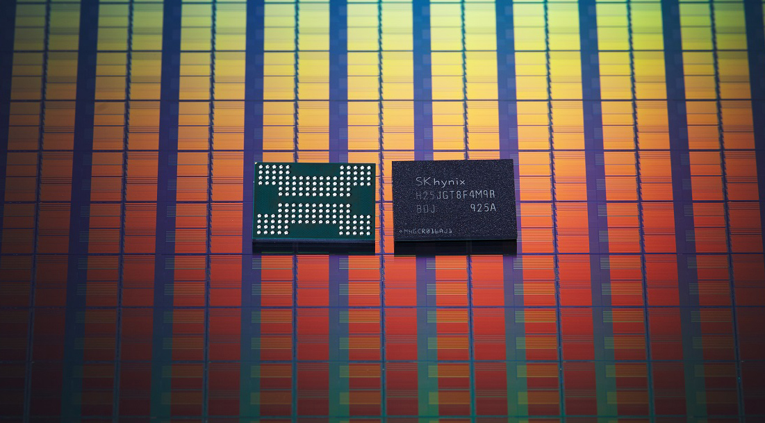
SK Hynix has announced it has finished development of its 128-layer 1 terabit 3D TLC NAND flash. The new memory features the company’s charge trap flash (CTF) design, along with the peripheral under cells (PUC) architecture that the company calls ‘4D’ NAND, announced some time ago. The new 128-layer TLC NAND flash devices will ship to interested parties in the second half of this year, and SK Hynix intends to offer products based on the new chips in 2020.
1 Tb 128-Layer ‘4D’ TLC NAND
SK Hynix’s 1 Tb 128-layer TLC NAND chip features four planes as well as a 1400 MT/s interface at 1.2 Volts. The quad-plane architecture along with a 1400 MT/s I/O bus will make the new TLC NAND devices not only significantly denser (in terms of Gb per mm2) than previous-generation products, but also at least 16% faster. In fact, real-world performance increase could be even higher as SK Hynix once said that its CTF design would enable a faster program time (tPROG) as well as a faster read time (tR).
To stack 128 layers inside its 6th Generation 3D NAND chips, the company had to use a multi-stacked design along with numerous new technologies, including ultra-homogeneous vertical etching technology as well as high-reliability multi-layer thin-film cell formation technology. Meanwhile, to increase performance of the I/O bus without increasing power consumption of the device, SK Hynix implemented its ultra-fast low-power circuit design.
It is noteworthy that transition to CTF + PUC architecture, along with various optimizations, enabled SK Hynix to reduce the number of process steps by 5% as well as increase bit productivity per wafer by 40% when compared to 96-layer TLC NAND. As a result, we should expect to see the new NAND run through the entire product lineup in due course.
Various Applications
SK Hynix and its partners will use the company’s 1 Tb 128-layer TLC NAND chip for a variety of applications.
“SK Hynix has secured the fundamental competitiveness of its NAND business with this 128-Layer 4D NAND,” said Executive Vice President Jong Hoon Oh, head of global sales & marketing. “With this product, with the industry’s best stacking and density, we will provide customers with a variety of solutions at the right time.”
Initial 1 Tb 128-layer TLC NAND chips that SK Hynix will start shipping in the second half of the year will be used primarily for mobile storage devices, such as USB drives and memory cards.
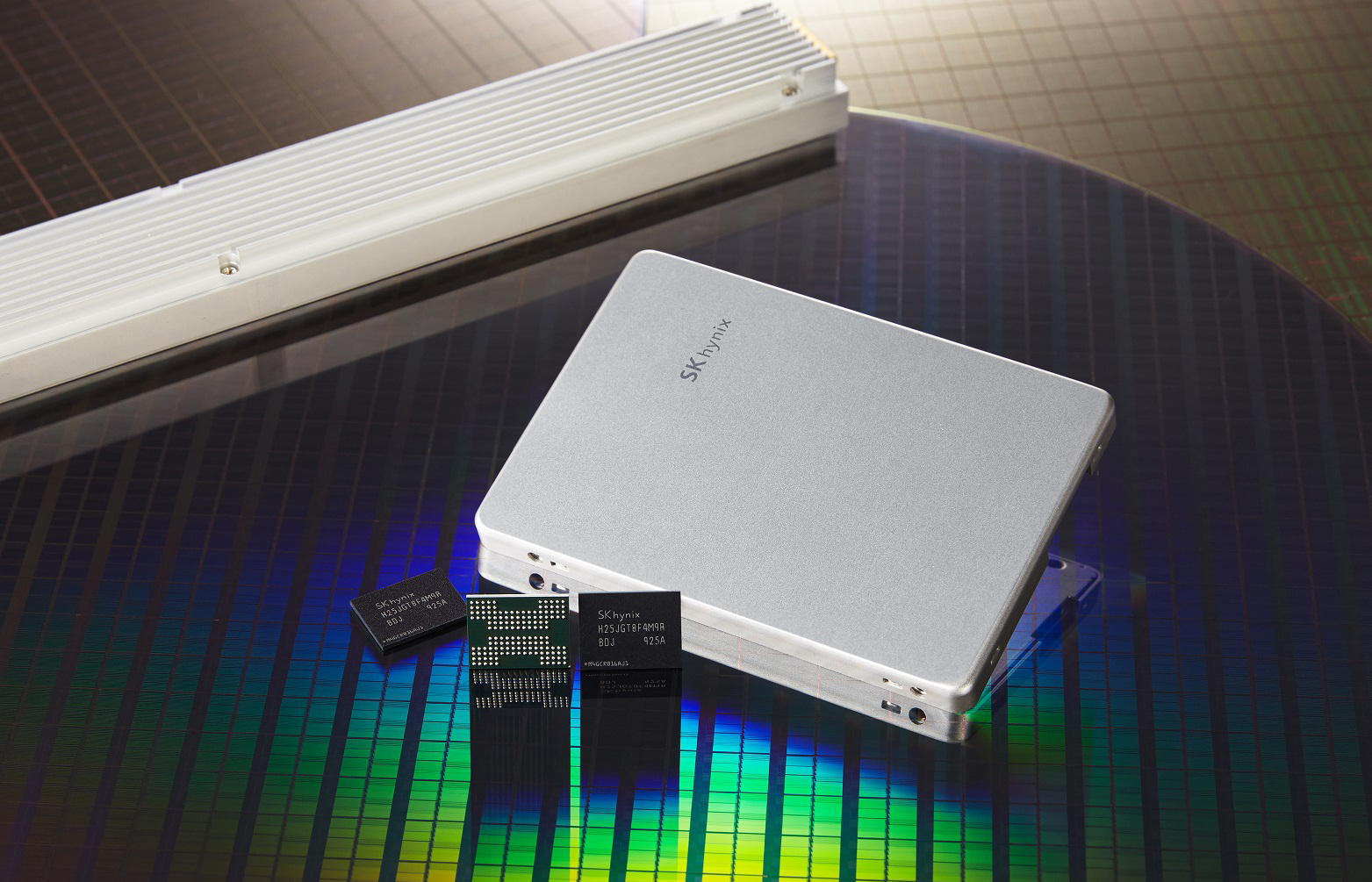
In the first half of next year SK Hynix promises to roll out its UFS 3.1 storage products based on the new 1 Tb devices. The company plans to offer 1 TB UFS 3.1 chips that will consume up to 20% less when compared to similar products that use 512 Gb ICs.
Later in 2020, SK Hynix intends to offer 2 TB client SSDs based on its own controller, as well as 16 and 32 TB server SSDs for datacenters ,.
176-Layer 4D NAND Incoming
String stacking technology, as well as the multi-stacked design, will enable SK Hynix to keep increasing the number of layers. SK Hynix says that it is currently developing 176-layer 4D NAND flash, but does not disclose when it is expected to become available.
Related Reading
- Flash Memory Summit 2018, SK Hynix Keynote Live Blog: NAND Development
- SK Hynix Begins Sampling of 96-Layer 1 Tb 3D QLC NAND
- SK Hynix Launches 96-Layer 3D NAND and Discloses QLC Plans
- SK Hynix Announces SSDs with 72-Layer 3D NAND ICs, Own Controllers
- SK Hynix Launches 2nd Gen Enterprise SSD: 72-Layer 3D NAND & In-House Controller
Source: SK Hynix


28 Comments
View All Comments
Santoval - Friday, June 28, 2019 - link
"In general terms 3D means 3 dimensional, 4 means 3D plus time"Not necessarily. 4D may also mean 4 spatial dimensions. Mathematicians casually play with 4D cubes, spheres and toruses, and they always mean 4 spatial dimensions (time is a concept in physics and some applied math; it does not really exist in pure math).
Spunjji - Thursday, June 27, 2019 - link
I was with you on 4D being a silly marketing term, but there's nothing "inevitable" about improvement in this area. Both of those descriptions cheapen the solid engineering effort that went into this.theeldest - Thursday, June 27, 2019 - link
IMFT (Intel and Micron) have been doing the CMOS under the Array since early 2016--more than 3 years ago.So it's ridiculous for SK to talk like they're the first ones to come up with *4D NAND*.
So it was inevitable given they knew their competition was doing the same thing to good effect.
nandnandnand - Thursday, June 27, 2019 - link
The other companies are working on string stacking, Western Digital has 1 Tb and 1.33 Tb NAND, etc. So yes, it is inevitable, and I'll cheapen it all day long.PeachNCream - Wednesday, June 26, 2019 - link
It must be packed with flux capacitors or something.RU482 - Wednesday, June 26, 2019 - link
what exactly is the 4th dimension in this NAND?philehidiot - Wednesday, June 26, 2019 - link
Time.They pull this crap with ultrasound machines. We have 2D and 4D imaging. 3D doesn't exist because it has a temporal component. This logic doesn't apply to the 2D button though, for reasons known only to cocaine addled spewers of marketing wank.
ksec - Wednesday, June 26, 2019 - link
NAND is interesting, on one hand we want to highest density and lowest cost, performance doesn't matter because its closest rival HDD doesn't even compare. On the other hand we want something that is crazy fast.I wish we could see $100 2TB SSD for bulk storage, even if it is QLD. I could then get a 4TB SSD NAS + 4TB 2.5" HDD as Backup.
Although we need 10Gbps Ethernet or 5Gbps Prices to drop first.... : /
Stochastic - Wednesday, June 26, 2019 - link
We'll get there before too long. You can already purchase 1 TB SSDs for under $100, so it's only a matter of time before you'll be able to get 2 TB at that price point.Spunjji - Thursday, June 27, 2019 - link
I was about to say the same thing. I chuckle every time I see these "I wish I could get x amount of NAND for y amount of money" comments, because every year x goes up and y goes down but z (the volume of grumbling) never changes. xD