An Interview with AMD’s Forrest Norrod: Naples, Rome, Milan, & Genoa
by Dr. Ian Cutress on June 24, 2019 8:00 AM EST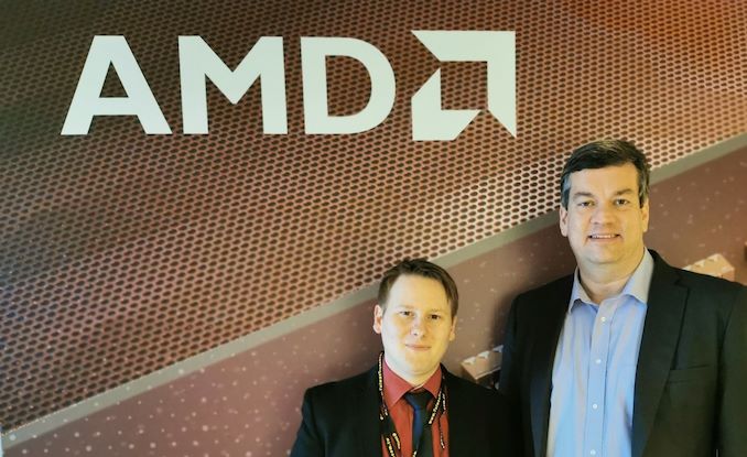
There’s no getting away from the fact that AMD’s big revenue potential exists in the server space. While the glitz and the glamor is all about the Ryzen, the big money is with EPYC. Heading up AMD’s EPYC efforts, as well as their extended collaborations in the embedded and semi-custom segments, is Forrest Norrod, the SVP and GM of the Datacenter and Embedded Solutions Group at AMD. We spent some time at Computex talking with Forrest about the upcoming premise of Rome, and how AMD now sees itself in the server and enterprise ecosystem.
 |
 |
| Forrest Norrod SVP & GM, AMD DESC |
Dr. Ian Cutress AnandTech, Senior Editor |
Also present was a journalist from PCWatch.
As with our interviews, we implement a refined transcription to benefit ease of reading, and also rearrange questions into segments.

Rome and the Future of EPYC
Ian Cutress: From our perspective we see Rome being the next step-up in AMD's revenues - as good as all the Ryzen and Zen 2 announcements for the consumer market, combined with the argument is consumer market is flat to declining, every competitor is trying to chase the same overall volume, but higher ASPs. By contrast, how do you see the enterprise market growing as AMD looks forward to bringing out Rome in Q3?
Forrest Norrod: We are super excited, so from our perspective Naples was always about reintroducing ourselves to the business, the ecosystem, the customers, the partners, and building credibility that we were back in the game. We set relatively modest share gain ambitions for Naples, and we're pretty much on track to do what we thought we could do. From day one, I always said to the team that Naples doesn't matter if we don't deliver Rome, if we can't look at our customers and say Rome is on time. By the way, Rome doesn't matter if we don't look at our customers and say Milan is on time, or it doesn't matter if we don't tell customers that we're ready to deliver Genoa. I'm going to stop there because otherwise I'm going to giveaway code names we haven't said yet!
But for the removal of doubt, Genoa is the Zen 4 design. Here's an exclusive: the one after that is another Italian City. I know you're shocked. We always knew that having the regular cadence in the road map was extremely important, and so the strategy was to have Rome be a part that could further accentuate our throughput leadership, and to get rid of as many asterisks as possible in terms of single thread performance, memory latency, and so on. That was always the strategy. Then Milan was designed to further erase any asterisks that remain, so in thinking about it, in the original strategy, Milan was where we expected to be back to IPC (or better) parity across all workloads. That was the thought process to the strategy.
Even with Intel's road map delays, we have continued to execute within a quarter of when we said we were going to execute - we've always come out within one quarter of where we planned it 3 years ago. Milan is right on track as well, but Intel is not, and so the relative competitiveness of Rome is actually better than we had originally had planned. We're seeing tremendous excitement in our customer base around it, and I think that's really a function of it being more competitive, but it's also a function of the fact that our partners now believe us. Now AMD delivered the original part and it works, and it's good and it's quality, we can deploy it at scale. We told customers two years ago that we we're going to come out with Rome in the middle of 2019 and now we’re telling them that we’re going to come out with Milan at a certain point in time, and they believe us. That helps a lot that belief, that the proof points, the predictable execution are very important.
IC: When Naples was announced, early access partners and cloud providers got it first. It was still another two quarters until general availability, and what we're hearing out of our sources is that Rome would be on a similar cadence to that for a variety of reasons. Can you explain what AMD’s plan is here?
Forrest Norrod: No. I would say normally over the last 10 years that when a processor gets introduced, most of the OEMs have most of the platforms available for 30-60 days at least, for most. Some will have some platforms available later but some will have platforms available in 30-60 days but that's normal. Then they shipped volume to lead HPC and cloud customers maybe 3 or 4 months earlier. I'd say we're right on track for that. So we're going to introduce Rome in Q3, and we're anticipating pretty good availability at launch and within that 30-60 day window.
IC: Just to put into perspective, does AMD have enough FAE's* to support its customers?
(An FAE is a Field Application Engineer, whose duties may include assisting partners in system and product design.)
Forrest Norrod: That's interesting. What you might be hearing is that compared to the current situation with Naples, we probably have quadruple the requests for Rome. So the reality is there is so much interest in Rome, that we are turning away platforms ideas right now, and we have been turning away platforms for the last 6 months. But plotting it out in terms of the platforms that we are supporting, we’re going to see a doubling of platforms from Rome.
PCWatch: I saw that market research from Mercury shows that AMD has almost 2% of the market share in the server market. When do you expect to have double digit market share?
Forrest Norrod: We normally look at IDC rather than Mercury, because Mercury includes a whole bunch of add-on parts in there that go into embedded applications, which are don't think are representative of real server markets. So if you peel out IDC, or even Mercury on the standard parts, we're roughly 5%. I think on that basis, what we've said in the past is we think it's 4 to 6 quarters to get to 10%, from Q4 of last year. So call it Q4 to Q2 next year.
Some Core Facts
PCWatch: With the upcoming Rome CPUs, are they compatible with the Naples platform?
Forrest Norrod: That's right - you can take a Rome, and you can take your existing Naples platform, and you can drop Rome in the Naples platform with a new BIOS and it'll work. However you will only have PCIe Gen3 and you'll have DDR4-2666. If you upgrade the platform and re-do the design on the I/O channels, then you can use PCIe Gen4. So it's very similar to what we do on the client side as well. We aren’t stating the memory speed, but you do get more than DDR4-2666.
PCWatch: For the upcoming Rome platform, how about the amount of the memory? The Naples platform is up to 2TB per socket, but how about Rome? Will it be over double, and will you support the new ICs from Samsung (and Micron)?
Forrest Norrod: Rome will support more, both in memory speed and in memory capacity.
PCWatch: Support for DDR5?
Forrest Norrod: DDR5 is a different design. It will be on a different socket. We've already said Milan is a mid-2020 platform, and we've already said that's socket SP3, so DDR4 will still be used for Milan.
Frontier and Semi-Custom Solutions
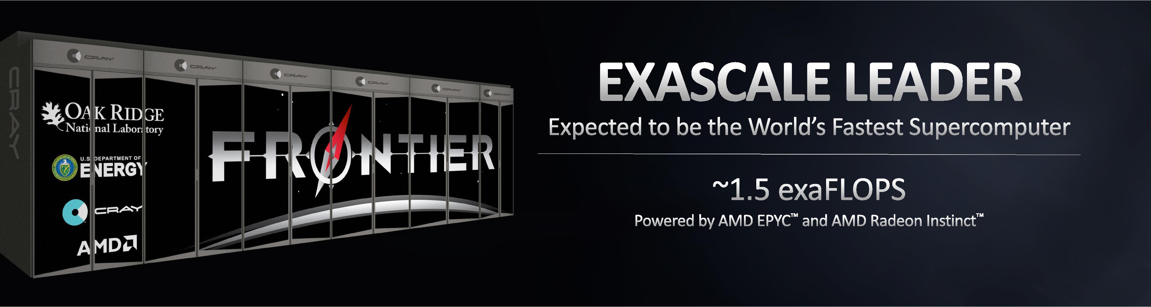
PCWatch: For the Frontier supercomputer, powered by AMD, is that using the Milan platform? With that processor, and with NVIDIA as a GPU*, Frontier, is a brand new system, but I can’t understand the current remarks on the CPU. Is it Zen 3?
Forrest Norrod: Frontier is not Milan. It’s a custom CPU.
*It should be noted that Frontier uses AMD GPUs, not NVIDIA GPUs.
IC: When Intel says they have a custom CPU, all they are doing is changing the core count, frequency, the cache, and perhaps the TDP. Are you using custom CPU in the same context?
Forrest Norrod: Intel talks big about having custom CPUs for the cloud guys and it's just different TDPs or configurations. When I say we are going to use a custom CPU for Frontier, that is not what I mean. Under Intel’s definition, we already supply custom CPUs, for example, Amazon needed a different model so we provided it to them - you can't buy it anywhere else. But no, when I say custom CPU, I mean it's a different piece of silicon.
IC: Would you classify it as coming from the semi-custom division?
Forrest Norrod: You know, there's a blurred line there, the some of the semi-custom resources are working on it. Here's one way to put it - we slot engineers around between the semi-custom group and the Datacenter and Embedded Solutions Group.
PCWatch: AMD disclosed that the Infinity Fabric is being used between the CPU and GPU. Is it going to become the common interface topology?
Forrest Norrod: Again, the thing about Frontier is I don't want to say anything to that level of specificity about something that is 2 years out. So let me hang onto that. It is a true statement with regards to Frontier that we use Infinity Fabric to connect the CPUs and the GPUs together, as well as GPU to GPU. We have also stated that Frontier is one CPU and four GPUs per system.
PCWatch: CCIX seems very suitable for connecting between the CPU and GPU, but in Frontier, but you're not using CCIX, you're using Infinity Fabric. Why are you not choosing CCIX?
Forrest Norrod: CCIX is a good interface, but was designed as a general purpose interface and is a standard. Defining standards requires you to accommodate a wide variety of devices on both sides of the wire. If you want to go for maximum performance, and can guarantee specific connectivity between two parts, you can increase the performance, but it won’t be a standard connection. And so the Infinity Fabric interconnect between the CPUs and the GPUs is lower latency, higher bandwidth, and it adds a number of attributes to really maximise the performance of that machine. But it's not a standard, you couldn't easily hook another device up to that.
IC: Is there anything about the Stadia that you'd like to tell us that we don't already know? Or do we have to ask Google?
Forrest Norrod: You would really have to ask Google. I'll say just as a gamer myself that when we first started talking to Google, and there were plans for a streaming game service, it was interesting, it was exciting and all that, but as you know the idea was not particularly new. But we were excited because the time may have finally come when we can do this properly. I'd say that as a gamer, when I first learned the completeness and the vision they have, that it wasn't just a streaming game service - they have rethought the social aspects of gaming. Also, if you decide to only write games that only work in a cloud gaming environment, it can be extremely fine-tuned. The completeness and vision of Stadia in the way that you can find the games, play the games, interact with the games, and totally new ways to do that - I think that's the most powerful thing about it. The graphics technology is cool and all that, but I got to hand props to Google on really thinking through those aspects.
PCWatch: Instinct is based on 7nm, so how about changing to the Navi architecture and performance?
Forrest Norrod: There's going to be some overlap between the two. I think Lisa eluded to this earlier, where GCN and Vega will stick around for some parts and some applications, but Navi is really our new gaming architecture so I don't want to go beyond that. You'll see us have parts for both gaming applications and non-gaming applications.
Power, Packaging, and Storage Class Memory
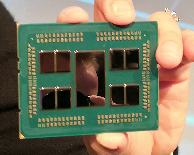
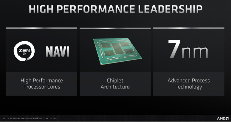
IC: With the new CPUs, and looking from Rome to Milan to Genoa, AMD is obviously going to use the chiplet design and leverage it to its full. Obviously the push to more and more performance is going to be borne out through not only IPC but also cores and that in turn involved a lot of interconnect, and that's what we're seeing the Infinity Fabric is slowly becoming half if not more than the power consumption of these chips. How does AMD manage that going forward?
Forrest Norrod: You know, I don't think it's that high so I don't want to give you that number, but it’s not that high. But certainly interconnect on a multi-die architecture is a significant concern. We do build our own PHYs to make sure that we're optimising the performance and the pJ per data transition. Then there's other things that are factored in, like channel capacitance and general characteristics. So you know you should expect to see us continue to evolve all aspects of the system package and chipset architecture to try to continue to manage power, while continuing to increase performance.
The thing that I will readily admit is every watt of power you're spending on something that's not the CPU, could be spent around the CPU core. So we do completely believe that managing power is the absolute proof. Actually very early on when I first got to AMD, I said to the power management group that they’re not the power management group they are the performance management group. Because the managing power in every other aspect and being able to divert that power to clock frequency in the CPU is the whole performance gain.
IC: So how is AMD investigating innovative packaging technologies?
Forrest Norrod: We continue to look at all of these aspects to make sure that we're pushing the technology forward.
PCWatch: In the future roadmaps, you have no plan to use 3D packaging technology?
Forrest Norrod: We already use traditional 2.5D in GPUs, and you should expect us to continue use it. I gave a talk at a university a couple of months ago and said at that talk that we're pushing forward on all sorts of packaging innovation. But you have to go up as well. But going up is not a panacea - if you stack, depending on how you stack, you can create thermal and power delivery issues. There are a large range of interesting problems that have to be solved.
IC: Intel has extended out to all the other aspects of the enterprise market in order addressing more TAM than ever before, because that is the goal for investors. One of those aspects is volatile memory and Optane. What can AMD do in this space, or is it worth it the customers that you're going for to do some sort of non-volatile memory?
Forrest Norrod: With all these forms of NVM I do think that there are two value propositions that people have been talking about.
One is the non-volatile aspect, to blur the lines between memory and storage, and customers will get much better large memory database machines etc. On the whole non-volatile aspect, I think people are doing the software work to enable that on a broader range of applications, but at the end of the day, the fact that you still have a failure domain at the node level means that the value is relatively smaller. Before you can commit, you're going to trust a commit to just one machine, to the SCM on one machine. However realistically you're not going to commit until you got a commit on multiple nodes. And so, that tends to somewhat degrade the value that people were thinking about.
So the other aspect of course is lower cost per bit. They’ll use it as DRAM replacement and the fact is that it has longer latency and non-uniform latency, and so there are a bunch of issues there. Now withstanding that it is close enough that we can use it as DRAM replacement, I'd say there was probably more interest in that 12 months ago when DRAM price were at a historically high level. Today there is less interest in that now as DRAM prices have come way down and I do think that DRAM/memory is a commodity market, and commodity markets have a very set of economic rules. The cure for high oil prices is high oil prices right? You know because that increases production and that brings the oil prices back down. The prospect of Optane being a replacement for DRAM in of itself would bring the cost of DRAM down, regardless of the current market factors in play today.
But there are a lot of other storage class memory (SCM) technologies which are in development. I think that you will see SCM settle into a niche of the memory hierarchy over 2-3 years and I think that there will be a lot of choices, not just Optane. But I don't think it's the be-all and end-all. I think that that Intel has made a horrific mistake hitching their system architecture to a propriety memory interface. I think that they've made a key strategic mistake.
I think that in general, Intel may be forgetting what got them here. Truly having an open ecosystem where others could add value to that ecosystem, and that the platform is a key part of the success of the x86 market. Intel still talks about it in that way, but that's not what they are doing, any pico-acre of silicon that doesn't belong to Intel is something that they covet. But I think acting that way is to the detriment of the health of their platform ecosystem long term.
Many thanks for Forrest and his team for their time. Also thanks to Gavin Bonshor for the transcription.
Related Reading
- Naples, Rome, Milan, Zen 4: An Interview with AMD CTO, Mark Papermaster (Q4 2018)
- An Exclusive Media Interview at AMD Tech Day, with CEO Dr. Lisa Su (Q1 2018)
- Making AMD Tick: A Very Zen Interview with Dr. Lisa Su, CEO (Q1 2017)
- An AnandTech Exclusive: The Jim Keller Interview
- Talking Snapdragon: An Interview with Cristano Amon, President of Qualcomm
- An Interview with Lisa Spelman, VP of Intel’s DCG
- Interview with Rod O’Shea, EMEA Embedded Group Director and Site Manager for Intel UK
- Interview with Jackson Hsu, Product Management Director at GIGABYTE


48 Comments
View All Comments
Kevin G - Tuesday, June 25, 2019 - link
That idea has been floated around as part of the custom nature of Frontier's CPU.As for HPE, they are one of the few with an Intel chipset license which was inherited when they purchased SGI. It is how they are able to build a 32 socket Xeon right now.
Doing something different with AMD for the more commodity parts is kinda difficult. AMD hasn't left many options open. Technically Rome should scale to quad socket merit of how many IF links there are and how many IO dies would be at play. It just isn't clear if AMD even has support for this. Vendors can build dual socket Rome boxes with 160 and 192 active PCIe lanes for accelerators now.
I am also curious if there is a Vega 20 card put into a Rome system if it would be possible to switch from PCIe to IF over the existing physical link That would be an interesting play for AMD.
Opencg - Monday, June 24, 2019 - link
I think just like people who simplify things down to "what node is it on" you are missing the point on chipplet strategy. AMD has used the appropriate chiplet approach on all of its products. This isn't the place for you to vent your feelings about ryzen chiplets in the form of garbled logic. Get your mind right.Oliseo - Tuesday, June 25, 2019 - link
Projecting much?Kevin G - Tuesday, June 25, 2019 - link
I would disagree in that we have yet to fully see the full benefits of AMD's chiplet strategy. So far they only have two IO dies where they put a selective amount of CPU dies into the same package. Not a bad start but far from its full potential.Need to move to PCIe 5.0 and/or DDR5? Only the IO die needs be changed. Need to add a GPU to make it a full mobile SoC? Link a GPU die to the IO die via IF without having to redesign the CPU or IO portions that have already been in production for months. Need to add fabric for a super computer? Link it the IO die via IF at the cost of a CPU die in the same package.
The chipset strategy is more than just being able to mix process nodes (for the record that is a good thing too, and I would also cite the ability to combat poor foundry yields for the amount of silicon being used as a third major benefit). It is about being able rapidly re-use what works with minimal validation to quickly produce custom products to fit market demands. We are only in the beginning stages of this strategy.
jamescox - Thursday, June 27, 2019 - link
The mobile part will probably be a single die APU. Where power consumption is the most important, there is still an advantage in having everything on one die. I don’t know how they will launch that since they already have 12nm APUs marketed a Ryzen 3000. Perhaps the 7nm mobile APU will be the first Ryzen 4000 part with desktop Ryzen 4000 parts (Zen 2+) coming a bit later.The main benefit of the chiplet strategy is the yields and the lower cost (they aren’t separate obviously). Intel can’t really compete with Ryzen 3000 parts with 14 nm parts. AMD will have a $200 part with 32 MB L3 and a $500 part with 64 MB L3. Intel 14 nm currently only goes up to 38.5 MB and those are expensive chips. Some of that is 7 nm vs intel 14 nm but having two or 3 chiplets is actually a really big part of AMD’s advantage. Intel will eventually get a 10 nm die on the market, but it will almost certainly still be a monolithic die. That will waste 10 nm die area on IO and also, a monolithic die with a lot of cores will be quite a bit larger and therefore lower yields than AMD’s tiny chiplets. If the competing intel part comes out at maybe 250 square mm, then that is going to be a lot more expensive than AMD’s 2 80 square mm chiplets (much better yields) and a cheap 14 nm IO die.
The comparison is even worse for intel with Epyc. Intel has their two die 56 core marketing part with 2 x 38.5 MB L3 cache, but being on 14 nm it consumes way too much power and it is ridiculously expensive. AMD has about 1000 square mm of silicon for a 64-core Epyc. You get a massive 256 MB L3 cache which intel doesn’t even come close to. The intel part is, I believe, 2 almost 700 square mm die, so around 1400 square mm total and probably bad yields due to the size. A 64 core part just cannot be done as a monolithic die. Even 2 die is still probably not doable on 10 nm due to worse yields.
So while it is true that they can mix and match parts with using separate die, that really isn’t that important. What is important is that it allows a 16 core desktop part for $749 while slower intel parts go for 2 to 3x that cost. Same thing with Epyc. The intel parts are ridiculously more expensive and at this point, Intel doesn’t even have a real competitor beyond 28 core. The dual 28 core parts are more marketing than real products. AMD is probably planning a new cpu chiplet for the DDR5 time frame anyway. I don’t know if they want to support both DDR4 and DDR5 in the next generation, but that would probably be easily possible by just making a new IO die while keeping compatibility with the old one. That would be great if they can do that but it isn’t why people are excited about Ryzen 3000.
Gondalf - Wednesday, July 3, 2019 - link
You have well underlined the advantages of chiplet design; too bad you have forgotten to underline the disasvantages on performance. This is very common, AMD too do this mistake.All server cpus suppliers avoid carefully the granular AMD solution, even ARM server suppliers are all on monolithic solutions. This is an indication that disavantages are bigger than advantages.
IMO AMD could have shipped a least a 16 core die for Epyc to reduce the insane amount of off die interconnection. I suspect that Rome will perform well only for a selected number of workloads.
I don't think Intel is concerned too much with Rome arrival.
deltaFx2 - Thursday, July 4, 2019 - link
@Gondalf: It is a tradeoff, but "This is an indication that disavantages are bigger than advantages" was true; not anymore. Intel is also doing multi-die packaging with Cooper/Ice lake based on rumors and have plans to use EMIB-based solutions in future (Sapphire Rapids). The reality is that latest and greatest nodes are taking longer to achieve yield parity with older nodes. You then have two choices: wait a couple of years for yields to catch up such that you can build a high core-count server part OR do what AMD is doing. So, the tradeoff AMD is making is that the extra cost (power, latency) from MCM is offset by power efficiency of 7nm. And when 7nm can yield a monolithic 32c die, AMD can jump to 5nm or whatever is the next node. More cores per socket, less power per core even when adjusted for the extra power from MCM.Plus, the argument that this is a bad idea because nobody else does it is a pretty weak argument. Nobody made $600 phones before Apple tried.
By all accounts that I have heard, AMD is gaining significant traction in cloud and HPC with Rome. The cloud folks run VMs or containers with few threads in each so don't really need a large unified cache that Intel provides (the biggest -ve for AMD). Basically what is called 'scale-out'. Then there's legacy enterprise ('scale-up') where AMD may be at a disadvantage (oracle, SAP databases). These workloads have a large number of threads with coherent shared memory. Whether this matters in the real world is hard to say. Clearly AMD has decided that it can ignore legacy database markets and focus on cloud, which is what, 40-50% of server volume?
deltaFx2 - Thursday, July 4, 2019 - link
PS: Naples had an additional wrinkle of being NUMA and apps running on it had to be NUMA-aware. This is not the case with Rome.jamescox - Thursday, June 27, 2019 - link
“Leveraging interposers does lower power consumption vs. traditional wire bonding that is used in the Rome packaging.”I don’t think actual wire bonding has been used for cpus in about 20 years; the Pentium Pro in the late 90’s was the last wire bonded Intel chip, I think. They moved to flip-chip with the Pentium 2 or perhaps a second revision of the Pentium 2.
I don’t think they will have ridiculously large silicon interposers. Interposers are made the same way silicon chips are so they are limited by the reticule size. Techniques do exist to make them larger than that, but the cost probably skyrockets. I would guess that the most likely configuration is to place gpus with HBM on separate interposers and then connect them with infinity fabric through the PCB. They probably want a large gpu and 4 stacks of
HBM for each gpu which is quite large. Although, for HPC 2 smaller gpus often perform the same as one larger GPU with 2x the compute and 2x the bandwidth, so it is unclear how big the gpus actually are and how many HBM stacks they will use. They will probably have the gpus and cpus mounted on a single board though. It is a lot easier to route 3 IF connections to each interposer with them on the same board.
The next step for Epyc seem to be to replace the IO die with an interposer. I don’t know if that will be Zen 4 though. It may come later. Using an interposer would allow using multiple much smaller 7 nm chiplets for the actual logic. An active interposer would be even better since they could place the larger transistors needed for driving off interposer links in the interposer and reserve the 7nm chips just for logic. Using an interposer for the IO die would allow better power consumption since the logic would all be 7 nm chiplets. An active interposer would free up a lot of extra area on the Epyc package. That could allow things like memory controller chiplets with very large caches on die and such. They could also move things around again and do something like place cpu cores and memory controllers onto one interposer and all of the other IO onto another chip since it isn’t as latency sensitive. An active interposer with the external memory interface would be interesting. Such a device might have 7 nm chiplet(s) with the memory controller and the IF switch and the cpu core chiplets on a single interposer. That would probably be pushing the reticule size limits with a passive interposer though. Even if the reticule size limits aren’t an issue, what if something goes wrong soldering the chiplets onto the interposer? Four gpus, a bunch of HBM, cpu chiplets, and possibly a bunch of other chiplets would be a lot to lose in one soldering operation.
There are a lot of different options once silicon interposers come into play, but I would still expect that they would use separate interposers for each gpu and the cpu and just connect them together with infinity fabric. If the cpu uses a silicon interposer then one possible customization is to place the slingshot interface directly on the interposer. If it is using an active interposer, then it could actually be the exact same chiplets as a regular Epyc with just an added die for slingshot and/or a different interposer with slingshot integrated.
Carmen00 - Monday, June 24, 2019 - link
Good interview, thank you! I wish that Mr Norrod was a bit more forthcoming in some areas, but what can you do...Some small typos caught my eye. "Lisa eluded to this earlier" should be "Lisa alluded to this earlier". "commodity markets have a very set of economic rules" ... is there a word or so missing here? "I think that that Intel has made" should be "I think that Intel has made".