TSMC Reveals 6 nm Process Technology: 7 nm with Higher Transistor Density
by Anton Shilov on April 17, 2019 9:00 AM EST- Posted in
- Semiconductors
- EUV
- TSMC
- 6nm
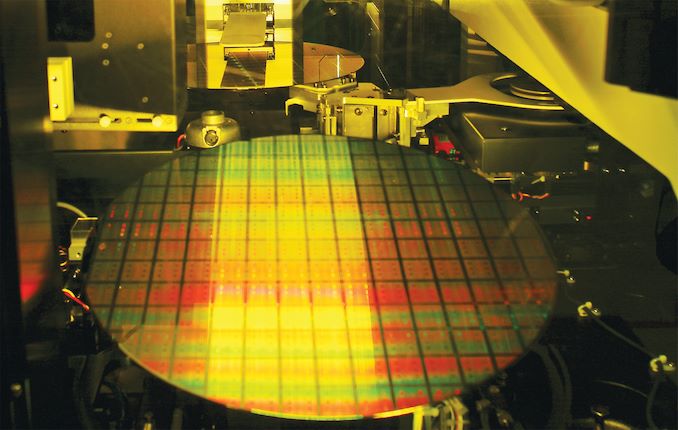
TSMC this week unveiled its new 6 nm (CLN6FF, N6) manufacturing technology, which is set to deliver a considerably higher transistor density when compared to the company's 7 nm (CLN7FF, N7) fabrication process. An evolution of TSMC's 7nm node, N6 will continue to use the same design rules, making it easier for companies to get started on the new process. The technology will be used for risk production of chips starting Q1 2020.
TSMC states that their N6 fabrication technology offers 18% higher logic density when compared to the company’s N7 process (1st Gen 7 nm, DUV-only), yet offers the same performance and power consumption. Furthermore, according to TSMC N6 'leverages new capabilities in extreme ultraviolet lithography (EUVL)' gained from N7+, but does not disclose how exactly it uses EUV for the particular technology. Meanwhile, N6 uses the same design rules as N7 and enables developers of chips to re-use the same design ecosystem (e.g., tools, etc.), which will enable them to lower development costs. Essentially, N6 allows to shrink die sizes of designs developed using N7 design rules by around 15% while using the familiar IP for additional cost savings.
| Advertised PPA Improvements of New Process Technologies Data announced by companies during conference calls, press briefings and in press releases |
|||||||||
| TSMC | |||||||||
| 16FF+ vs 20SOC |
10FF vs 16FF+ |
7FF vs 16FF+ |
7FF vs 10FF |
7FF+ vs 7FF |
6FF vs 7FF |
5FF vs 7FF |
|||
| Power | 60% | 40% | 60% | <40% | 10% | ? | 20% | ||
| Performance | 40% | 20% | 30% | ? | same (?) | ? | 15% | ||
| Area Reduction | none | >50% | 70% | >37% | ~17% | ~15% | 45% | ||
TSMC says that it expects N6 to be used for a variety of applications, including mobile SoCs, GPUs, high-performance computing chips, networking, 5G infrastructure, and other products. What remains to be seen is whether chip designers will be inclined to use N6 technology given its miniscule improvements over N7 when it comes to power, performance, and area (PPA). Perhaps, companies with complex N7-based chips will prefer to go directly to N7+, or even 5 nm (CLN5FF, N5), for their next generation parts.
TSMC will start risk production of chips using its N6 fabrication technology in the first quarter of 2020. Keeping in mind that it usually takes companies about a year to start high-volume manufacturing (HVM) after the beginning of risk production, expect N6 to be used for mass products starting from 2021.
Related Reading:
- TSMC’s 5nm EUV Making Progress: PDK, DRM, EDA Tools, 3rd Party IP Ready
- TSMC: 7nm Now Biggest Share of Revenue
- TSMC: First 7nm EUV Chips Taped Out, 5nm Risk Production in Q2 2019
- TSMC Details 5 nm Process Tech: Aggressive Scaling, But Thin Power and Performance Gains
Source: TSMC


23 Comments
View All Comments
Yojimbo - Saturday, April 20, 2019 - link
From the earnings call, there's a little more information on the N6 node, but it's still confusing. It's coming out later than N7+ and its performance and density specs seem to be similar to N7+. TSMC say they expect customers to move from N7 to N6 and not use N7+. And I got the idea there seems to be some disappointment on the characteristics of N7+.In some ways it seems like a replacement for a disappointing N7+, though I'm not sure if that's accurate or not. It also is going to be coming available around the time N5 is coming available. I am guessing TSMC expect high end smartphones to use N5 and higher-powered leading-edge compute to use N6. One more thing, TSMC said that N6 will use one more layer of EUV than N7+ and they also said something about learning from their N7+ experience when creating N6.
Here is on of the quotes by the CEO from the conference call:
"As we continue to improve our 7-nanometer technology and by leveraging the EUV landing form, N7+, we now introduce N6 process. N6 has three major advantage. First, N6 have 100% compatible design rules with N7, which allows customer to directly migrate from N7-based design, which substantially shorten the time-to-market. Second, N6 can deliver 18% higher logical density as compared to N7 and provide customer with a highly competitive performance-to-cost advantage. Third, N6 will offer shortened cycle time and better defect density. Risk production of N6 is scheduled to begin in first quarter year 2020 with volume production starting before the end of 2020."
My guess is the third advantage is the advantage that N6 holds over N7+, regardless of whether a company is using N7 already or not. I am inferring that perhaps N7+ has proved to have long cycle times and/or high defect density. So the cost of N6 should be much less for big power-hungry chips. In other words, big GPUs
A couple more relevant quotes from the CEO on the issue:
"As I said, we have a very high tape-out activity for N7 for this year. Actually, a lot of customer from the [indiscernible], and mostly is from the HPC area, they are all designing their product with N7. A few of them has adopted N7+. But then that’s why we introduced our N6 that can be 100% compatible to the N7. So I’ll give you a taste of that probably starting year 2020. Most of the customer in the N7 will move to N6. And from that beyond probably, the N6 will pick up all the momentum and pick up all the volume production."
So N6 will pick up what would otherwise be N7/N7+ volume in 2021. N7+ will be skipped by all but a few customers. N7 customers will mostly move to N6 rather than N5 in that time frame. So it sounds like TSMC expect N7 in 2019 and 2020 and N6 in 2021, with only a few customers using N7+.
"Right. The question is about N6. It looks like N6 is behind N5 in terms of schedule. So what is the application? Well, again, I want to reiterate that N6 is coming from the N7, N7+ experience, learning. And so the N6, if you – a lot of customers are already entering N7 with a lot of tapeout. So N6 provide them a very good task that they can easily put in their current product into N6. So gain the benefit of either the performance, the tie area and also the shortened cycle time. N5 is a totally new node."
Yojimbo - Saturday, April 20, 2019 - link
So, it sounds to me like GPUs will use N7 and N6 and not N7+. N6 sounds like a way of reducing the cost of big, complex chips, exactly the thing the GPU manufacturers are looking for, similar to what the 12FFN node seemed to be. So, for example, perhaps NVIDIA will introduce an N7-based GPU in 2020 and then an N6-based GPU in 2021 or 2022.Adonisds - Sunday, October 27, 2019 - link
How much does it cost to make a factory ready to print 7nm chips? How much would it cost to make the factory ready to print the same in 6nm, given that you already did the 7nm? How much cheaper is that compared to going 6nm for the first time?