TSMC Reveals 6 nm Process Technology: 7 nm with Higher Transistor Density
by Anton Shilov on April 17, 2019 9:00 AM EST- Posted in
- Semiconductors
- EUV
- TSMC
- 6nm
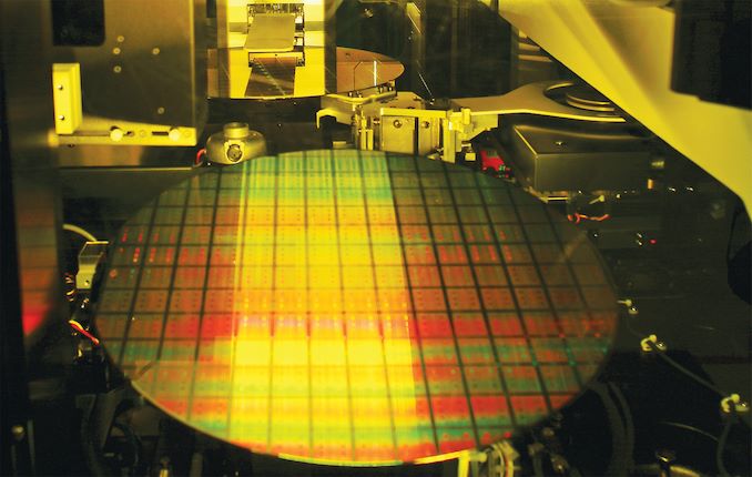
TSMC this week unveiled its new 6 nm (CLN6FF, N6) manufacturing technology, which is set to deliver a considerably higher transistor density when compared to the company's 7 nm (CLN7FF, N7) fabrication process. An evolution of TSMC's 7nm node, N6 will continue to use the same design rules, making it easier for companies to get started on the new process. The technology will be used for risk production of chips starting Q1 2020.
TSMC states that their N6 fabrication technology offers 18% higher logic density when compared to the company’s N7 process (1st Gen 7 nm, DUV-only), yet offers the same performance and power consumption. Furthermore, according to TSMC N6 'leverages new capabilities in extreme ultraviolet lithography (EUVL)' gained from N7+, but does not disclose how exactly it uses EUV for the particular technology. Meanwhile, N6 uses the same design rules as N7 and enables developers of chips to re-use the same design ecosystem (e.g., tools, etc.), which will enable them to lower development costs. Essentially, N6 allows to shrink die sizes of designs developed using N7 design rules by around 15% while using the familiar IP for additional cost savings.
| Advertised PPA Improvements of New Process Technologies Data announced by companies during conference calls, press briefings and in press releases |
|||||||||
| TSMC | |||||||||
| 16FF+ vs 20SOC |
10FF vs 16FF+ |
7FF vs 16FF+ |
7FF vs 10FF |
7FF+ vs 7FF |
6FF vs 7FF |
5FF vs 7FF |
|||
| Power | 60% | 40% | 60% | <40% | 10% | ? | 20% | ||
| Performance | 40% | 20% | 30% | ? | same (?) | ? | 15% | ||
| Area Reduction | none | >50% | 70% | >37% | ~17% | ~15% | 45% | ||
TSMC says that it expects N6 to be used for a variety of applications, including mobile SoCs, GPUs, high-performance computing chips, networking, 5G infrastructure, and other products. What remains to be seen is whether chip designers will be inclined to use N6 technology given its miniscule improvements over N7 when it comes to power, performance, and area (PPA). Perhaps, companies with complex N7-based chips will prefer to go directly to N7+, or even 5 nm (CLN5FF, N5), for their next generation parts.
TSMC will start risk production of chips using its N6 fabrication technology in the first quarter of 2020. Keeping in mind that it usually takes companies about a year to start high-volume manufacturing (HVM) after the beginning of risk production, expect N6 to be used for mass products starting from 2021.
Related Reading:
- TSMC’s 5nm EUV Making Progress: PDK, DRM, EDA Tools, 3rd Party IP Ready
- TSMC: 7nm Now Biggest Share of Revenue
- TSMC: First 7nm EUV Chips Taped Out, 5nm Risk Production in Q2 2019
- TSMC Details 5 nm Process Tech: Aggressive Scaling, But Thin Power and Performance Gains
Source: TSMC


23 Comments
View All Comments
stanleyipkiss - Wednesday, April 17, 2019 - link
This sounds like an nVidia "special node" ... just like the one developed for Turing.melgross - Wednesday, April 17, 2019 - link
It does seem to be coming after 7+, which will be available this year, in 2019. This is intermediate between 7+ and 5. So depending on cost, manufacturers will have a transition point in 2020, before 5 will be available, apparently, if all goes well, in 2021.After that, who knows? We read about 3nm, but will it really appear? Just a few years ago, most chip experts weren’t sure that 5nm could be achieved. Everyone has gotten over the 14nm hump, including Intel. But will there be a 3nm hump? Will 5nm come out on time? We don’t know the answer to either of those questions yet.
haukionkannel - Wednesday, April 17, 2019 - link
You have to remember that the so called 7nm product is not even near real 7nm size... It is purte marketing. So 3nm could really be 60nm in real size... because the marketing nm and real nm are so far away from each others...melgross - Wednesday, April 17, 2019 - link
Well, compared to what Intel does, it’s not. But the lines are 7nm, so that’s what we call it. The + labels are to show improvements, such as getting the lines closer together, improvements in sizing transistors, etc.Intel is denser, but the others are about, depending on methodology and capability, about one node looser, not ten, as you’re saying.
Wilco1 - Thursday, April 18, 2019 - link
Intel is certainly not denser. When they finally get 10nm out of the door, actual chips will have less than half the density of current 7nm TSMC chips.The nm number is just a number, however it does represent an ordering between processes, and in that sense the numbers are close to reality.
melgross - Friday, April 19, 2019 - link
That’s not true, but ok.peevee - Thursday, April 18, 2019 - link
"Just a few years ago, most chip experts weren’t sure that 5nm could be achieved."And it has not been. In reality, they are all more like 40nm+ with thinner wires for lower voltages.
Anymoore - Thursday, April 18, 2019 - link
Same design rules but higher density means it's not the lithography but track height change or diffusion break reduction.melgross - Thursday, April 18, 2019 - link
It doesn’t matter how it’s done. It’s all about minimizing wasted space.peevee - Thursday, April 18, 2019 - link
"Area Reduction:7FF+ vs 7FF ~17%
6FF vs 7FF ~15%"
Do I understand correctly that their "6FF" is actually LESS dense than their own 7FF+?