Cadence Tapes Out GDDR6 IP on Samsung 7LPP Using EUV
by Anton Shilov on November 26, 2018 3:00 PM EST
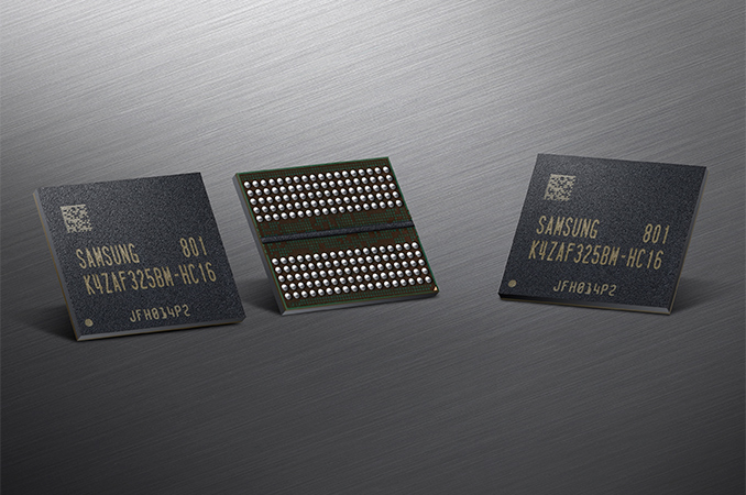
Cadence has announced that it has successfully taped out its GDDR6 IP on Samsung’s 7LPP fabrication process. The new building blocks should enable developers of various chips to be made using 7LPP and quickly and easily integrate support of GDDR6 memory into their SoCs.
Cadence’s GDDR6 IP solution includes the company’s Denali memory controller, physical interface, and verification IP. The controller and PHY are rated to handle up to 16 Gbps data transfer rates per pin and feature a low bit-error rate (BER) feature that decreases retries on the memory bus to cut-down latency and therefore ensure a greater memory bandwidth. The IP package is available as Cadence’s reference design that allows SoC developers to quickly replicate implementation that the IP designer used for its test chip.
Traditionally, GDDR memory has been used primarily for graphics cards, but with GDDR6 things look a bit different. Micron and a number of other companies are trying to drive GDDR6 to other applications as well. Apparently, they are not alone. Cadence says that its GDDR6 IP could be used for SoCs aimed at AI/ML, automated driving, ADAS, cryptocurrency mining, graphics, and high-performance computing (HPC) applications, essentially indicating interest towards GDDR6 from non-GPU developers. Meanwhile, being the world’s largest maker of DRAM, Samsung is clearly interested in adoption of GDDR6 by non-graphics applications.
Samsung’s 7LPP manufacturing technology is the company’s leading-edge fabrication process that uses extreme ultraviolet lithography (EUVL) for select layers. The tech is currently used to make an undisclosed SoC, but is expected to be used by a wider range of chips in the future. The GDDR6 IP from Cadence will naturally make 7LPP more attractive to designers of SoCs, but keep in mind that Samsung has a relatively limited EUVL capacity at the moment
Cadence’s GDDR6 IP is available now for customer engagements with design files ready for select clients.
Related Reading
- Samsung Starts Mass Production of Chips Using Its 7nm EUV Process Tech
- Arm and Samsung Extend Artisan POP IP Collaboration to 7LPP and 5LPE Nodes
- Samsung Foundry Roadmap: EUV-Based 7LPP for 2018, 3 nm Incoming
- Micron Begins Mass Production of GDDR6
- SK Hynix Lists GDDR6 Memory as ‘Available Now’, Publishes Final Specs
- Samsung Updates on GDDR6 Portfolio: 8 Gb and 16 Gb at Multiple Speeds
- Samsung Starts Mass Production of 16Gb GDDR6 Memory ICs with 18 Gbps I/O Speed
- Micron, Rambus, & Others Team Up To Spur GDDR6 Adoption in Non-GPU Products
Source: Cadence


11 Comments
View All Comments
Eric Klien - Wednesday, November 28, 2018 - link
Nvidia's V100 uses HBM2 running at 0.9 TB/s memory bandwidth. We're getting there!