TSMC Starts to Build Fab 18: 5 nm, Volume Production in Early 2020
by Anton Shilov on January 31, 2018 2:00 PM EST- Posted in
- Semiconductors
- SoCs
- EUV
- TSMC
- 5nm
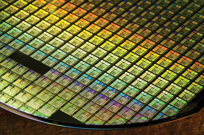
TSMC last week held a groundbreaking ceremony for its Fab 18 phase 1 production facility. The fab will produce chips using TSMC’s 5 nm process starting from early 2020. When all three phases of the manufacturing facility are completed, its wafer starts capacity will exceed one million 300-mm wafers per year, comparable with other three GigaFabs operated by TSMC.
TSMC’s Fab 18 will be located in Tainan (in the Southern Taiwan Science Park), and will be built in three phases. The construction of the first phase or segment of the building will be completed in about a year from now, after which TSMC will move in equipment sometime in early 2019. In about two years from now, the company expects to start volume production of chips using its 5 nm process technology at the Fab 18/phase 1. Construction of the second and the third phases will commence in Q3 2018 and Q3 2019. The two phases will start volume production in 2020 and 2021, respectively.
| TSMC's Fab 18: Milestones | |||||
| Phase 1 | Phase 2 | Phase 3 | |||
| Construction Start | Early 2018 | Q3 2018 | Q3 2019 | ||
| Equipment Move-In | Early 2019 | ? | ? | ||
| High-Volume Manufacturing Start | Early 2020 | 2020 | 2021 | ||
The Fab 18 will have a total floor area of 950,000 square meters and its cleanroom area will exceed 160,000 square meters, the contract maker of semiconductors said. TSMC estimates that the combined production capacity of all three phases of the Fab 18 will exceed one million 300-mm wafer starts per year, which is comparable to the capacities of the other GigaFabs that TSMC operates — Fab 12, Fab 14, and Fab 15. It is noteworthy that the planned floor area and cleanroom space of the Fab 18 will be significantly larger than the initially planned floor and cleanroom area of the Fab 15, which emphasizes increasing complexity of IC manufacturing these days as well as increasing orders from TSMC's clients. In total, the Fab 18 will cost TSMC NT$500 billion ($17.08 billion), making it one of the most expensive chip manufacturing facilities in the world.
| Brief Comparison of TSMC's Fab 15 and Fab 18 | ||||
| Fab 15 | Fab 18 | |||
| Total Area of Site | 18.4 hectares | ? | ||
| Building Area | 430,000 m² | 950,000 m² | ||
| Clean Room Space* | 104,000 m² | 160,000 m² | ||
| Initially Expected Investment** | NT$300 billion ~$9.375 billion |
NT$500 billion ~$17.08 billion |
||
| Groundbreaking | July 2010 | January 2018 | ||
| Notes | *Fabs are usually upgraded over time, today's cleanroom space of the Fab 15 may be larger than initially projected. **Initially expected investments tend to change over time. |
|||
Besides its dimensions and cost, there is another reason why Fab 18 is important for the semiconductor industry: it will be one of the world’s first facilities to produce chips using a 5-nm production tech. TSMC yet has to detail its 5 nm manufacturing technology, but from the announcements that the company has made so far it is evident that this fabrication process will rely significantly on EUV lithography. TSMC did not mention EUV at all in its press release, which is a bit strange. Meanwhile, over the course of last year the semiconductor manufacturer did mention that the 5 nm fabrication technology would be its second-gen EUV process, which means usage of EUV for more more layers when compared to the CLN7FF+ (its advanced 7 nm tech). Furthermore, TSMC already has functional SRAM cells made using its CLN5FF technology and the yields were satisfactory in mid-2017. Therefore, the 5 nm development process seems to be going on relatively well.
The extended usage of EUV for 5-nm chip production means that the company will need to install more EUV tools into the Fab 18, which is one of the reasons why it needed to expand the fab’s cleanroom space. The fact that TSMC has begun to build Fab 18 indicates that the contract maker of chips is confident in its 5 nm technology as well as EUV equipment, including ASML’s TWINSCAN NXE scanners, Cymer’s EUV light sources and other tools. This confidence is further underscored by their intention to start high-volume manufacturing of 5-nm devices in Fab 18 in early 2020.
| Advertised PPA Improvements of TSMC's CLN7FF Nodes Data announced by TSMC during conference calls, press briefings and in press releases |
||||||
| 7FF vs 16FF+ |
7FF vs 10FF |
7FF EUV vs 7FF |
5FF EUV vs 7FF EUV |
|||
| Power | 60% | <40% | 10% | lower | ||
| Performance | 30% | ? | lower | higher | ||
| Area Reduction | 70% | >37% | ~10% | tangible | ||
| HVM Start | ~Q2 2018 | - | ~H2 2019 | H1 2020 | ||
Related Reading:


26 Comments
View All Comments
Frenetic Pony - Wednesday, January 31, 2018 - link
Prediction: Production will begin in 2020. Sorry 2021. 2022. 2023, 24, 25, 26...FullmetalTitan - Thursday, February 1, 2018 - link
Kind of my thought, especially since they haven't secured EUV for use in their 7nm node. Unless ASML is magically doubling scanner production next year, they are currently on a 1 tool per month pace, most of which through 2019 have been pre-purchased by various foundries.Speedfriend - Monday, February 5, 2018 - link
FullmetalHas ASML published where their EUV machines are going?
Pork@III - Thursday, February 1, 2018 - link
I seriously worry about the lack of numbers in the row of "Performance"MrSpadge - Thursday, February 1, 2018 - link
Not your point to worry about right now. They will have some idea and probably data, but won't publish them yet (7 nm production has not even started!).Anymoore - Thursday, February 1, 2018 - link
Where has TSMC reported 5nm SRAM results? That should have been big.