Hot Chips: Google TPU Performance Analysis Live Blog (3pm PT, 10pm UTC)
by Ian Cutress on August 22, 2017 5:58 PM EST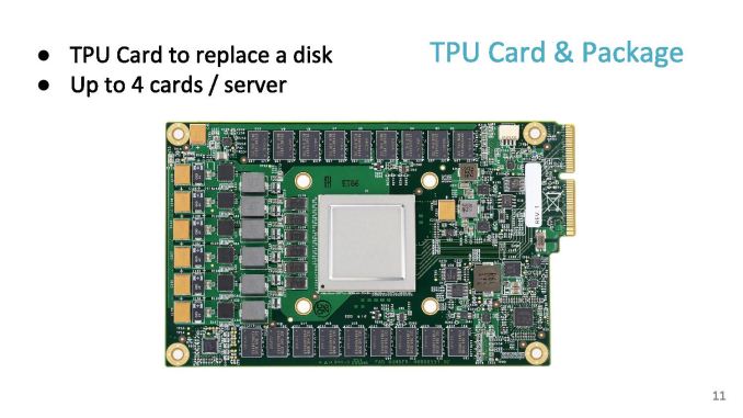
06:00PM EDT - Another Hot Chips talk, now talking Google TPU.
06:00PM EDT - TPU first generation is inference only accelerator
06:00PM EDT - 'Batch Size is an easy way to gain perf and efficiency
06:02PM EDT - TPU was a future looking product: in 2013, if everyone wanted to speak to their phone 2-3 minutes a day, it would take 2-3x current total CPU performance
06:02PM EDT - 'TPU project is an investment for when the performance is needed'
06:04PM EDT - Develop machine learning in terms of Tensor Flow, the idea is to make TPU easy
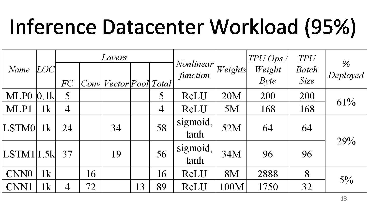
06:05PM EDT - After deploying convolutional neural network, it's interesting how small of our total workload it is
06:05PM EDT - TPU is an accel card over PCIe, it works like a floating point unit

06:06PM EDT - The compute center is a 256x256 matrix unit at 700 MHz
06:06PM EDT - 8-bit MAC units
06:06PM EDT - Peak of 92 T ops/sec
06:06PM EDT - DDR3 interfaces happen to be a bandwidth limit for the original TPU
06:06PM EDT - Not an ideal balanced system, but lots of MACs
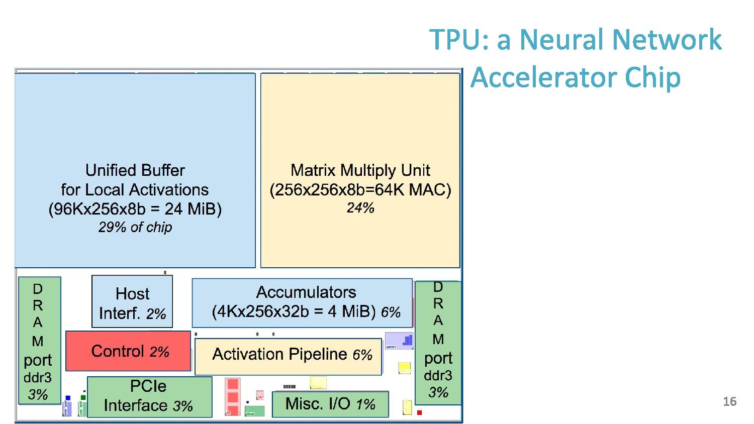
06:07PM EDT - Chip size, 30% for buffer, 24% for matrix unit

06:07PM EDT - Software instruction set has 11 commands, five of which are the ones mostly used
06:07PM EDT - Average 10 clock cycles per instruction
06:08PM EDT - Dispatch 2000 cycles of work in one instruction
06:08PM EDT - In order, no branching
06:08PM EDT - SW controlled buffers
06:08PM EDT - Hardware was developed quickly, difficulty shifted to software to compensate
06:09PM EDT - Problem: energy/time for repeated SRAM accesses of Mat mul
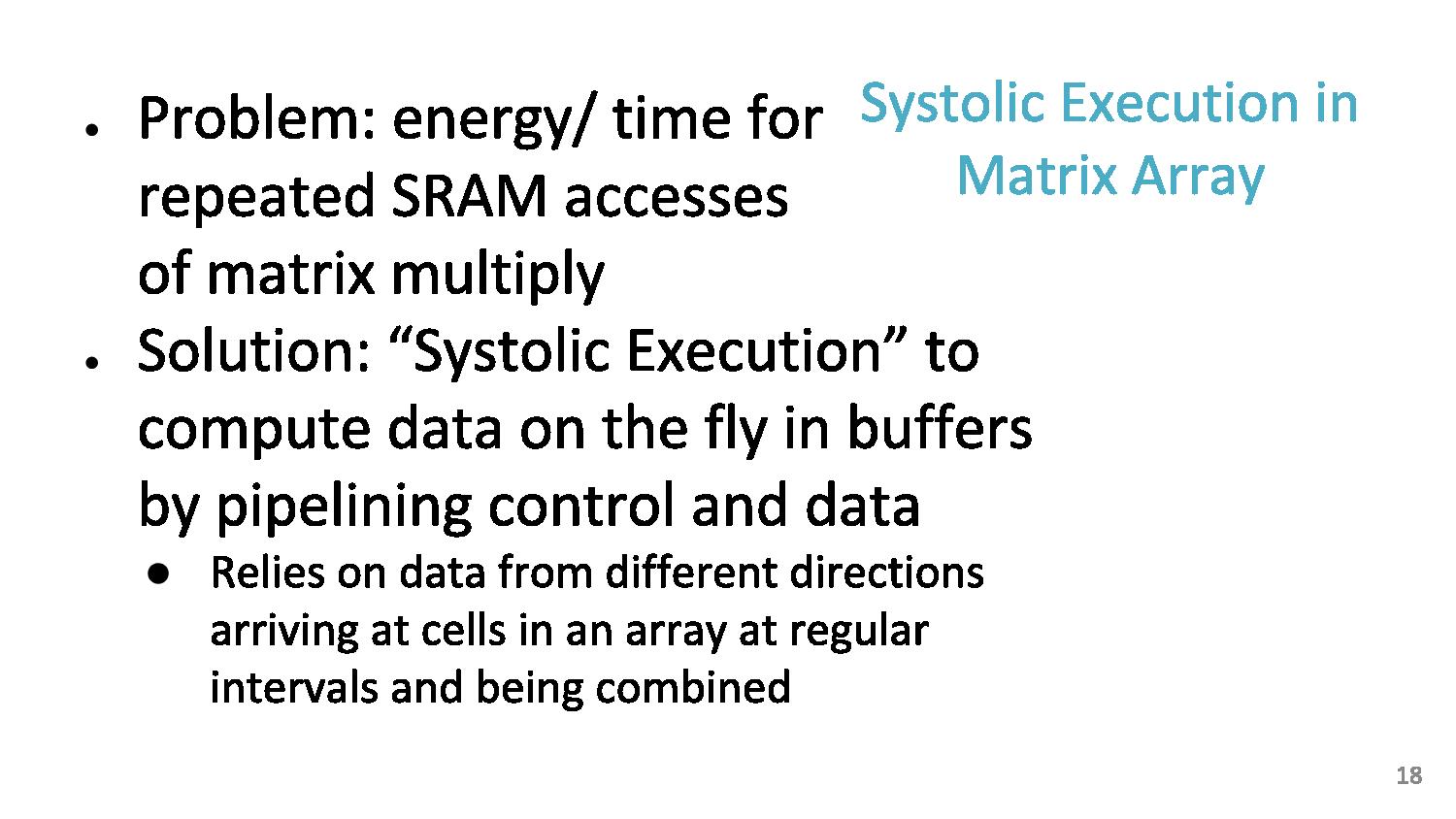
06:09PM EDT - As each input moves across the array, it gets multiplied, then added as it move down the array
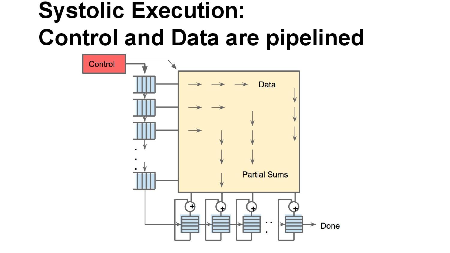
06:09PM EDT - Jagged timings, so systolic
06:10PM EDT - Can ignore pipeline delays by design
06:10PM EDT - First chips in datacenter in 2015, compared to Haswell and K80s
06:10PM EDT - Die size of TPU was smaller, TDP was smaller
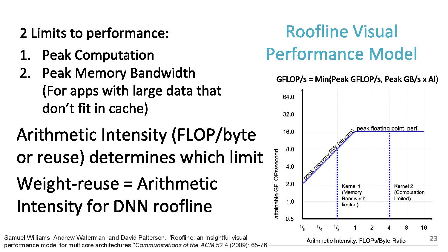
06:10PM EDT - 2 limits to performance: peak computation and peak memory (roof-line model)
06:11PM EDT - Arithmetic intensity (FLOPs per byte) determines which limit you hit
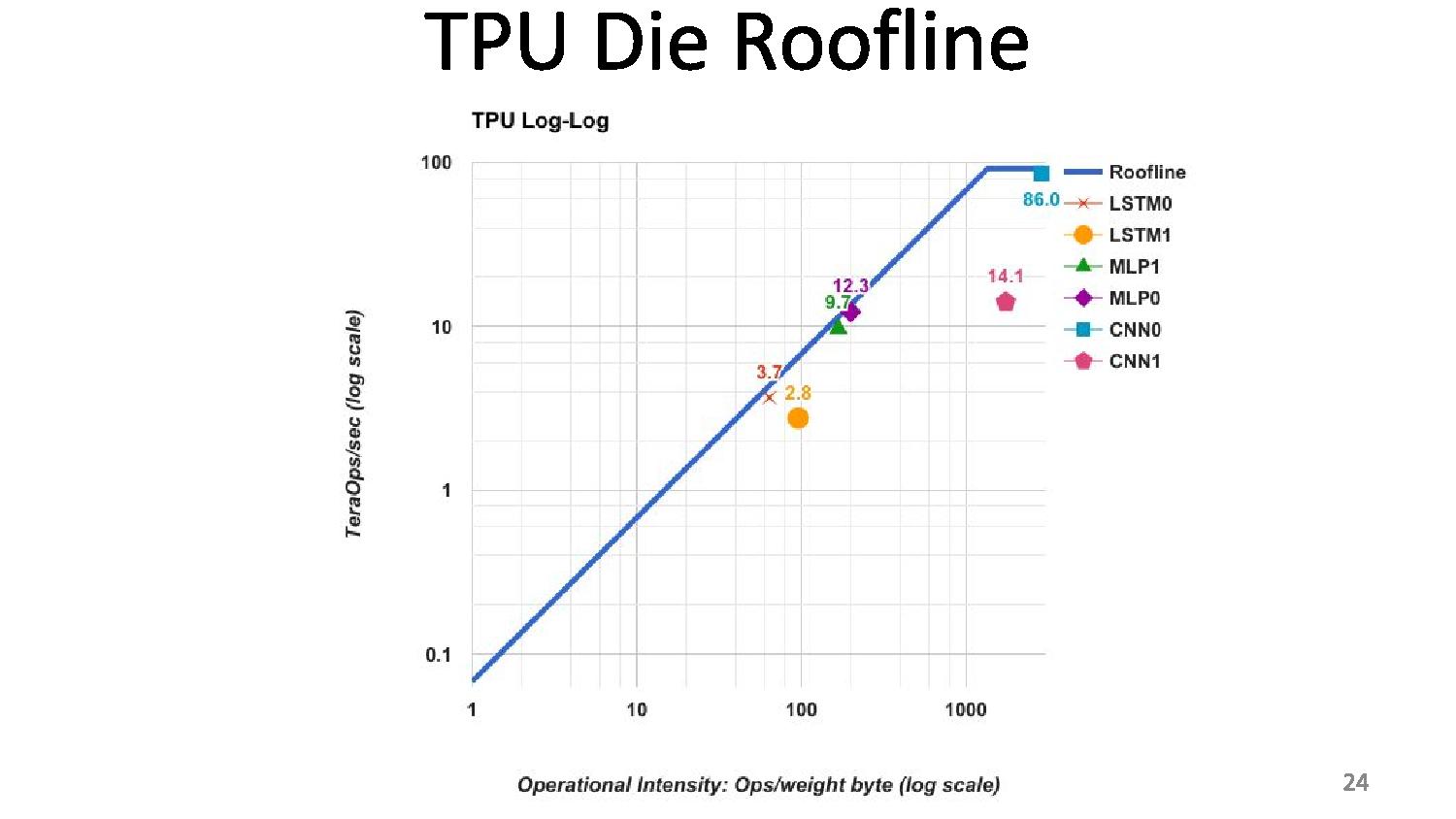
06:12PM EDT - TPU is near peak use in roofline, but only two tests hit the roofline. Other tests hit the memory limit
06:12PM EDT - We thought users would be in the inference cycle limit when first gen was developed
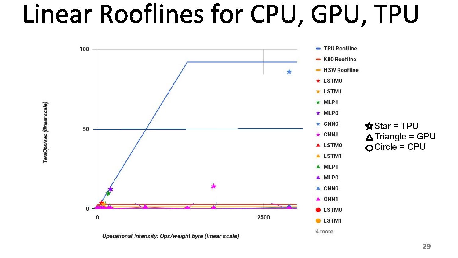
06:12PM EDT - CPUs and GPUs are better balanced, but performance are a lot lower
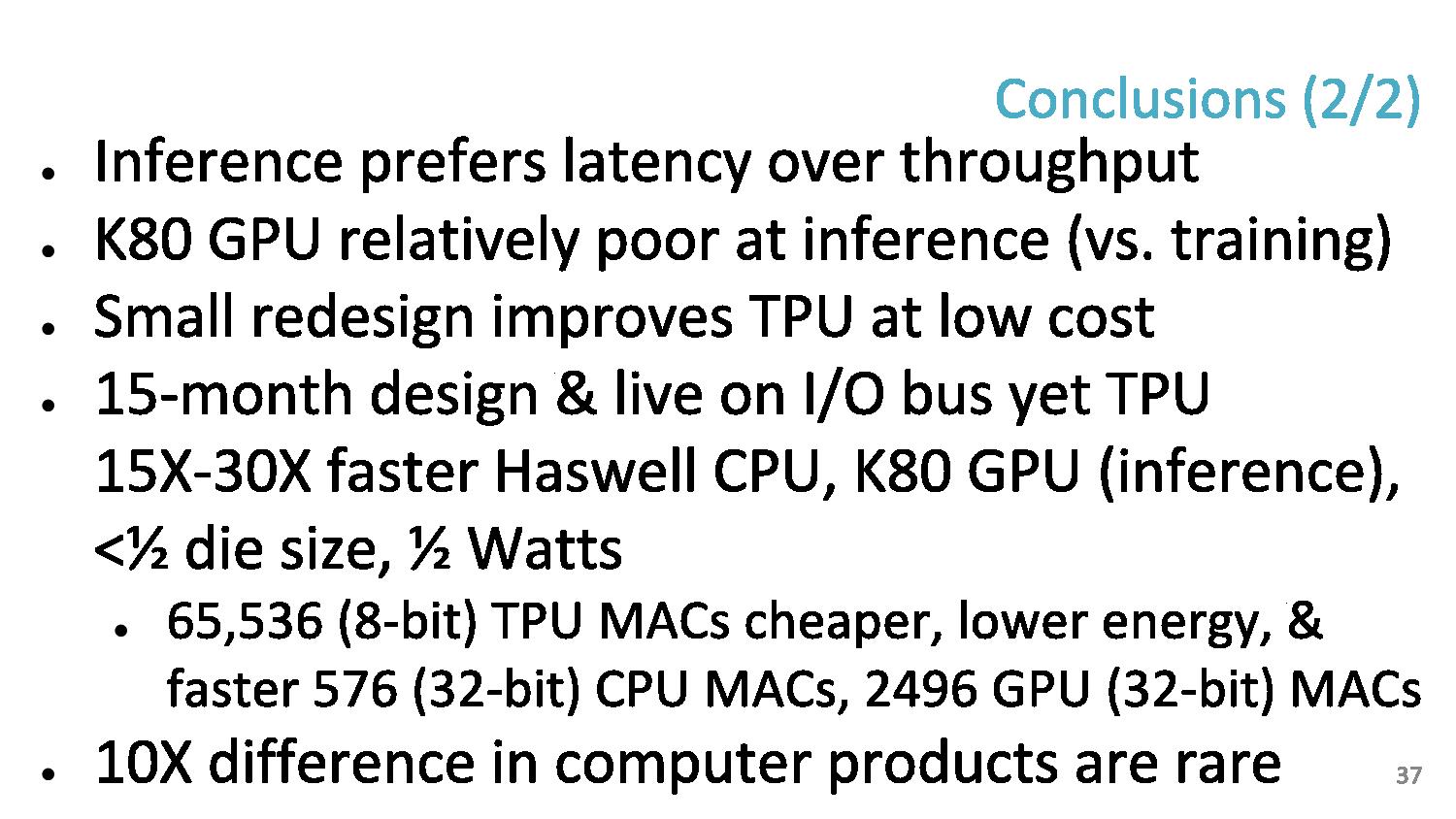
06:12PM EDT - We built a throughput machine, but it's being used in a latency driven manner

06:15PM EDT - Perf/watt 80x compared to Haswell, 30x compared to K80
06:15PM EDT - Roofline plot says memory limited
06:15PM EDT - So improving TPU: moving the ridge point
06:15PM EDT - Change 2x DDR3 memory to GDDR5 for example, due to memory limit. Improves performance for certain tests
06:15PM EDT - Ends up 200x perf/W over Haswell, 70x over K80
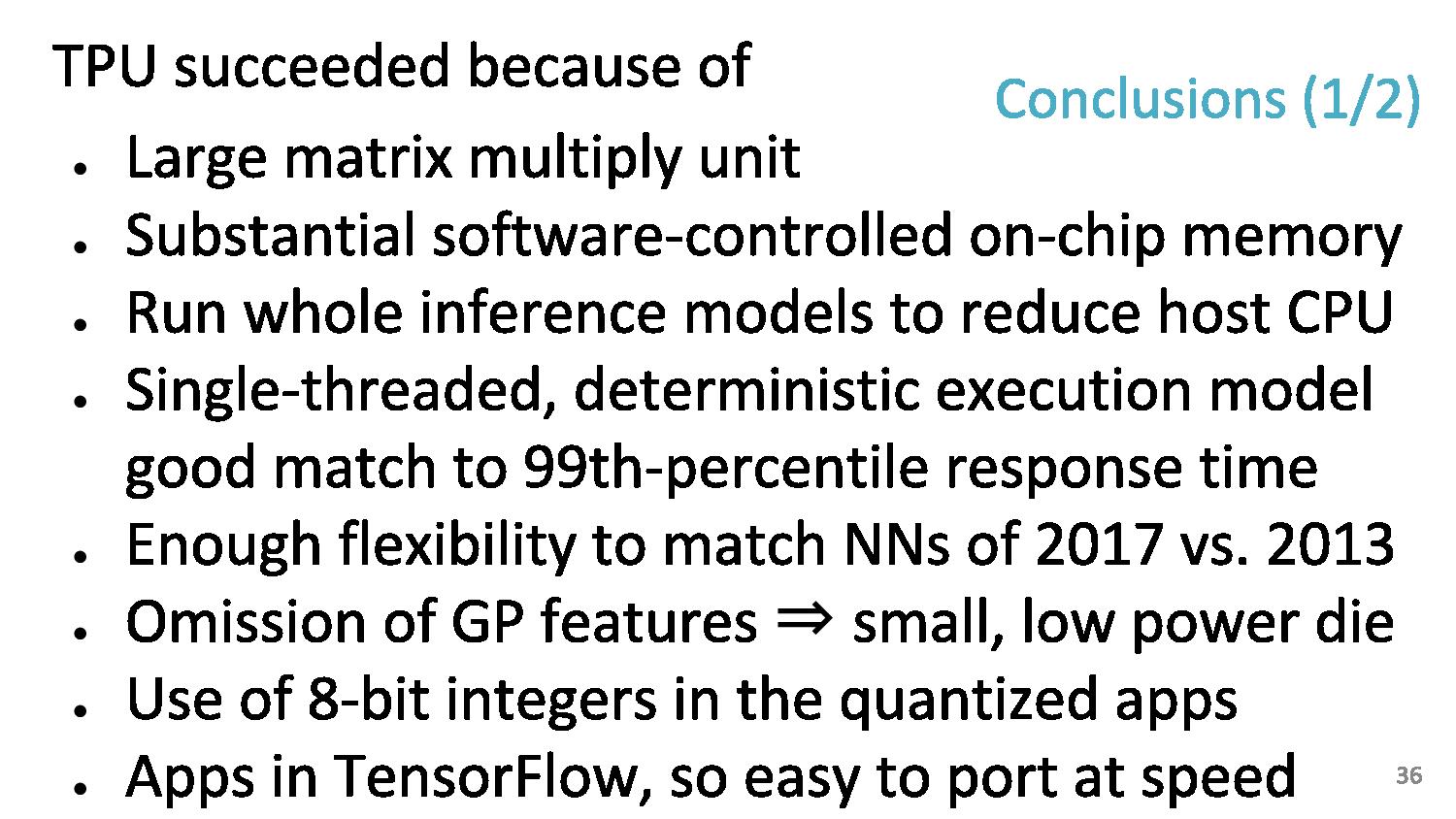
06:17PM EDT - At a top level, the TPU succeeds due to the exercise in application specific design
06:18PM EDT - At a top level, the TPU succeeds due to the exercise in application specific design
06:18PM EDT - As TPUs go forward, we will also get to do backwards compatibility to see how a machine ages
06:18PM EDT - Flexibility to match NNs in 2017 vs 2013
06:18PM EDT - Single threaded deterministic execturion model good match to 99th percentile response time
06:18PM EDT - Apps in Tensor Flow, so easy to port at speed
06:18PM EDT - When you have a large 92 TOPs hammer, everything looks like a NN nail
06:18PM EDT - Run the whole inference model on the TPU
06:18PM EDT - Easy to program due to single thread control, whereas 18-core CPU is difficult to think about
06:19PM EDT - Makes it easy to mentally map problem to single threaded environment, e.g. AlphaGo
06:20PM EDT - In retrospect, inference prefer latency over throughput - K80 poor at inference vs capability in training
06:21PM EDT - In the DRAM, a small redesign improves the TPU a lot (solved in TPUv2
06:21PM EDT - 65546 TPU MACs are cheaper than CPU/GPU MACs
06:21PM EDT - Time for Q&A
06:22PM EDT - Q: What is the minimum size problem to get good efficiency on the TPU - what is the right way to think about that
06:23PM EDT - A: I don't have a complete answer, but colleagues have mapped single layer matmuls and got a good payoff, but the goal is neural networks with lots of weights
06:23PM EDT - Q: Does the system dynamically decide to run on TPU over CPU
06:23PM EDT - A: Not at this time
06:24PM EDT - Q: Precision of matmul?
06:24PM EDT - A: 8-bit by 8-bit integer, unsigned and unsigned
06:24PM EDT - A: 8-bit by 8-bit integer, unsigned and signed
06:24PM EDT - A: 8-bit by 8-bit integer, unsigned and signed*
06:26PM EDT - Q: Does google view sparseness and ever lower precision
06:27PM EDT - A: 1st gen does not do much for sparse-ness. Future products not disclosed in this. Reduced precision is fundamental. We'd love to know where the limit for training and inference is in lower precision
06:27PM EDT - Q: TPU 1 had DDR3, and GDDR5 study got a lot performance, did you build a GDDR5 version?
06:28PM EDT - A: No, but the new TPU uses HBM
06:30PM EDT - Q: How do you port convolution to GEMM? A: Discussed in papers and patents! There's two layers of hardware to improve efficiency
06:32PM EDT - That's all for Q&A. There was a TPU2 talk earlier that I missed that I need to look through the slides of and write up later.
06:32PM EDT - .


30 Comments
View All Comments
Yojimbo - Tuesday, August 29, 2017 - link
You are underestimating the improvements in GPUs specifically for this task. What you are forgetting is that the K80 operated on 32 bit floats, whereas the P40 can operate efficiently on 8 bit integers. That allows 4 times the theoretical throughput without accounting for more cores or faster clocks. From the K80 to the P40, the GPU improved theoretical throughput over 6x for deep learning inference, with an improvement much greater than that if latency is taken into account.That's why the K80 was a dinosaur for these workloads and why trotting it out as a comparison in 2017 is only relevant for a historical perspective.
willis936 - Wednesday, August 23, 2017 - link
It looks like a big fat 8-bit ALU. Peak 92 trillion operations per second? When can I get one of these for NNEDI3 so I can watch my cartoons in upscaled 4K?shinpil - Wednesday, August 23, 2017 - link
Did google really say that precision of matmul is 8-bit by 8-bit integer?I think it is 8-bit by 8-bit float, not integer.
Google highlights high flops performance on slide, not integer.
Yojimbo - Wednesday, August 23, 2017 - link
Where do they? I only see it in the roofline model slide. That's just explaining the model. Unless I'm missing something, in the data graphs they call it TeraOps/sec. That's because the TPU was doing 8-bit integer operations and the GPU was doing 32-bit float operations. I forget what the CPU was doing, they noted it in their paper that they released last year.shinpil - Wednesday, August 23, 2017 - link
I have seen deep learning like CNN and DNN uses floating point operations not fixed point operations. So I confused.8 bit integer only covers -128~127.
I think this range is too narrow to handle lots of applications.
I wonder how google solved this problem.
Yojimbo - Thursday, August 24, 2017 - link
Well, actually researchers even make networks with 1 or 2 bits. 8 bit is generally not good for training because the gradient descent algorithm doesn't work too well with such low precision, I think. But researchers have had success with taking a trained network and quantizing it to represent the weights with 8 bit integers. Remember that there are millions of weights in a deep neural network. There is plenty of freedom to fit a target function with only a limited number of states for each weight.Nenad - Thursday, August 24, 2017 - link
It is INT8 for their first generation of TPU at least.You can see that in Google article that explain their 1st gen TPU in more details: https://cloud.google.com/blog/big-data/2017/05/an-...
They mention "we apply a technique called quantization that allows us to work with integer operations instead" ... but I think in their 2nd gen TPU, Google is using float ( https://www.nextplatform.com/2017/05/17/first-dept... )
Also, those comparisons with GPU on their slides are outdated - new NVidia Volta GPUs have tensor arithmetic integrated in GPU and achieve 120 TFLOPS , which is comparable even to new Google TPU2 which has 45 TFLOPS per module (or 180 TFLOPS per 'card' consisting of 4 connected modules )
p1esk - Friday, August 25, 2017 - link
So, Volta V100 chip does 120TFlops, while TPU2 chip does only 45TFlops. Not sure how Google is planning to compete.Yojimbo - Friday, August 25, 2017 - link
Well, one can't compare those peak theoretical numbers to get a good idea of how the various options perform. One needs to compare real world benchmarks. It's complicated because scalability and power efficiency play a part, as well.p1esk - Saturday, August 26, 2017 - link
You're right, the benchmarks is the only way to compare. Still, TPU seems to specialized for DL computation, while V100 does very well in FP32 and FP64 as well. Can you imagine how much faster V100 would be for DL if they fill its entire die area with "tensor cores"?