Intel Announces 7th Gen Kaby Lake: 14nm PLUS, Six Notebook SKUs, Desktop coming in January
by Ganesh T S & Ian Cutress on August 30, 2016 9:00 AM EST- Posted in
- CPUs
- Intel
- 14nm
- Kaby Lake
- Gen 9
- Speed Shift
- Turbo Boost
When Intel first announced the shift from the dual-stage ‘Tick-Tock’ methodology that had driven their core CPU design teams for over a decade into the three-way ‘Process, Architecture, Optimization’ paradigm, there were questions as to how much of the final stage, the Optimization, would actually change the way CPUs were presented or offer upgrades in performance. At the time, ‘Kaby Lake’ as the name for Intel’s third crack at their 14nm process was well known, but users wondered if it was just another Devil’s Canyon (better overclocking) or a full on CPU launch. Well the answer is the latter, and the launch is staggered between today and January. Roll on Kaby Lake. Is that Kah-bee Lake, or Kay-bee Lake?
Tick-Tock to Process-Architecture-Optimization (PAO)
Intel’s two year processor cadence of Tick-Tock allowed the company to alternate reducing the lithography node (a tick) with an upgraded microarchitecture (a tock) with modest gains of performance. Each stage of the Tick-Tock would take 12-15 months, with new lithography nodes taking longer and longer to reach maturity. Eventually it has gotten to a point where 14nm took too long to become pervasive in Intel’s product stack. For a manufacturing company and a CPU company, slowly rolling out Broadwell notebook and low power parts and then gutting the mid-range desktop was the result of the troubles of bringing 14nm to the prime time. Now in 2016 we have the launch of full-sized Broadwell-EP server parts running up to 22 cores in a 145W envelope, but the low power parts are a couple of microarchitectures ahead. We have this strange situation of a stretched landscape, partially driven by markets but also for manufacturing.
The move from Intel’s 14nm process to 10nm is a long, slow burn, taking much longer to develop than any process previous. We first saw 14nm in Broadwell mobile CPUs in Q3 of 2014, almost two years ago, and 10nm still isn’t on any public roadmap for early 2017. With the tick-tock strategy, and the launch of Skylake in mid-2015, this would leave Intel without a new CPU launch for almost two years, which is unheard of from Intel. Also, Intel’s partners rely on product cycles to announce and launch new products to generate revenue. To fill the gap, plus with a few other techniques, Intel moved to Process-Architecture-Optimization, or PAO for short.
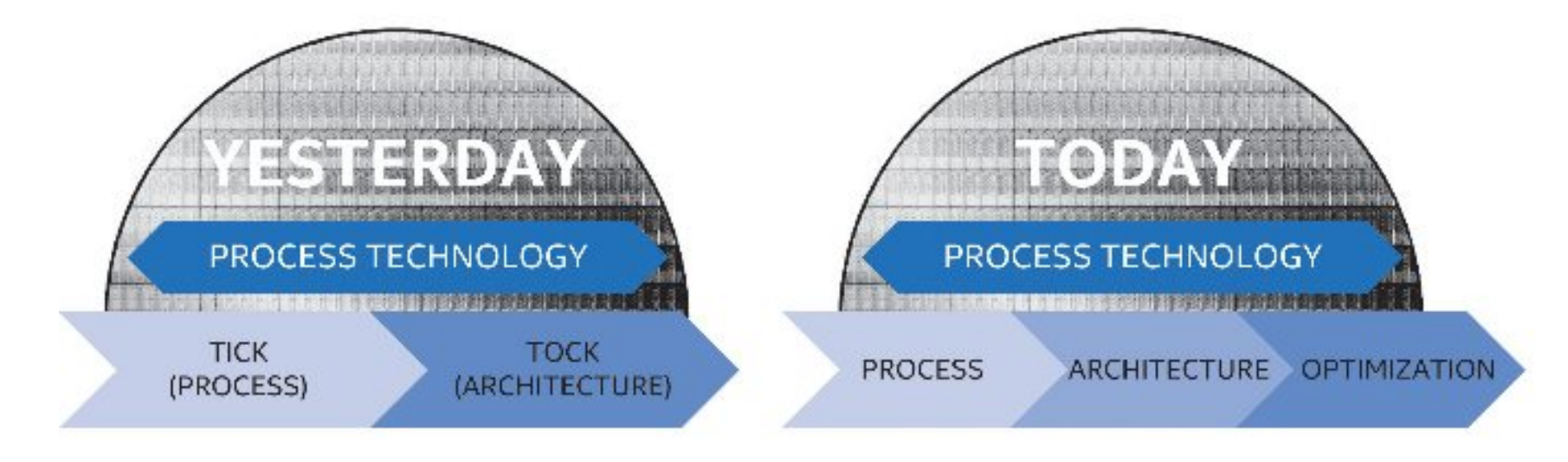
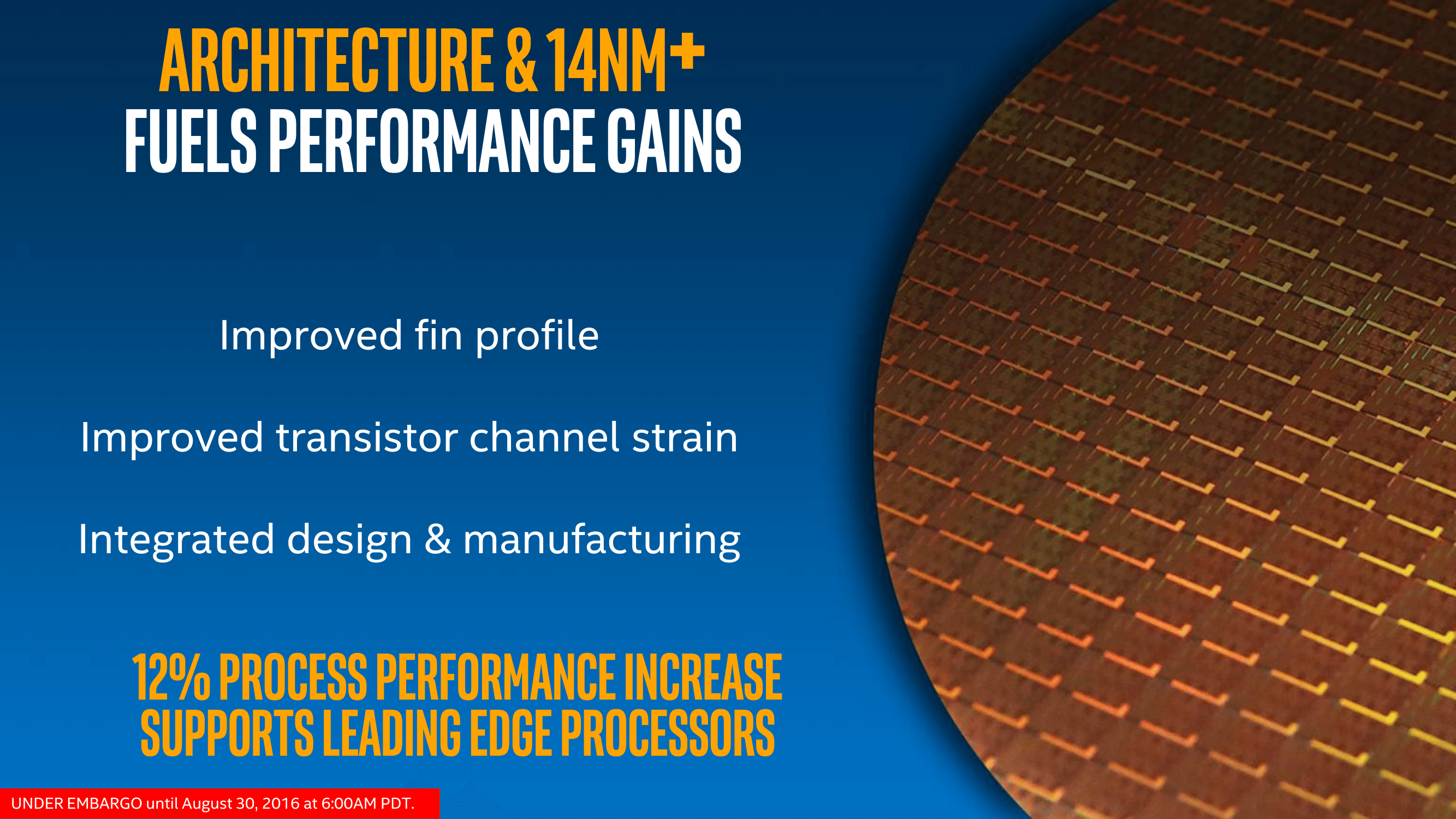
This means three bites of the cherry for 14nm before we see 10nm in prime time. First it was Broadwell, then Skylake, and today Intel is announcing Kaby Lake. As part of the release, Intel has mentioned that a number of key benefits for Kaby Lake will be based on an optimized 14nm process, called 14PLUS (or 14nm+, 14FF+). This process as a quick summary has a higher fin height and larger pitch, essentially giving a less-dense set of transistors that have more room to breathe. Normally a larger pitch means more voltage required, but this is offset by the fin height and Intel says is good for another few hundred MHz for performance. The less-dense design, in theory, may also help in overclocking, however we will have to wait until January to see those results.
Today’s Announcement
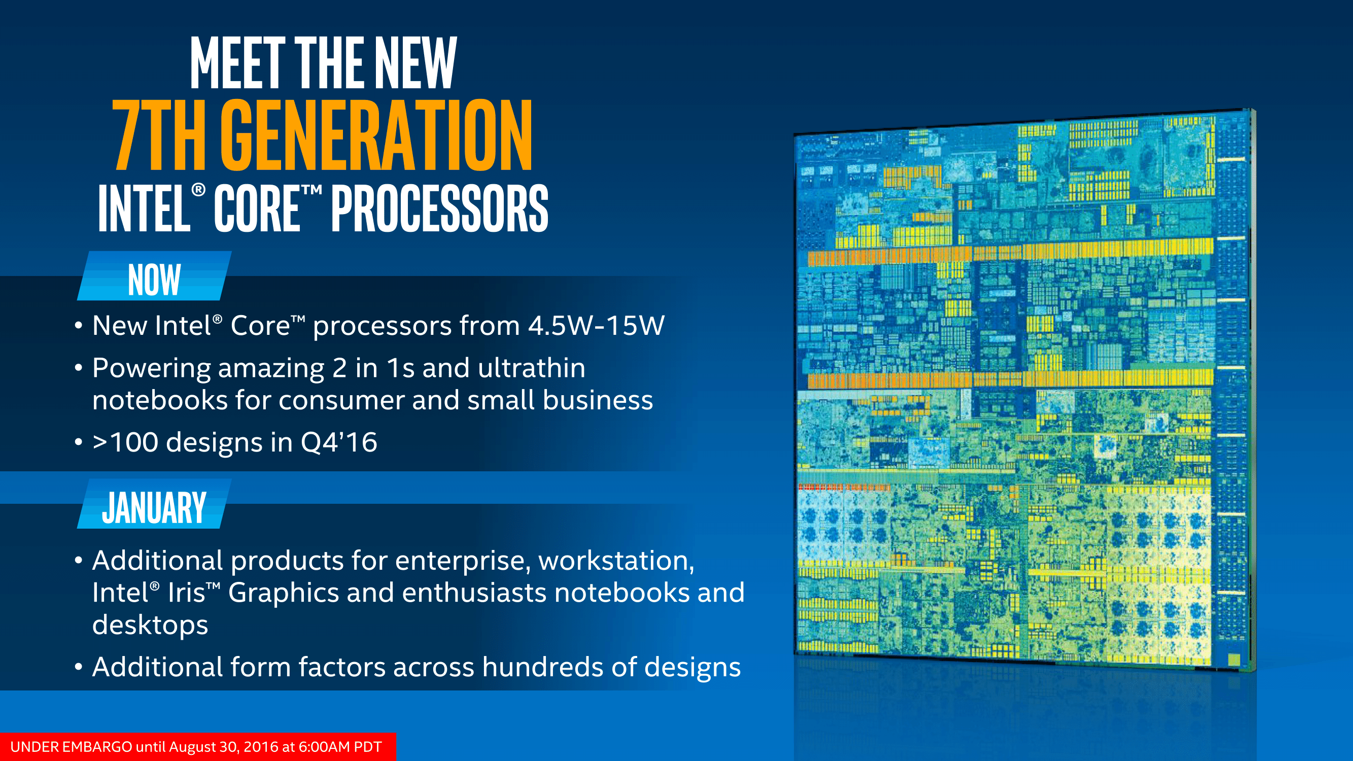
The reveal today covers several aspects of Kaby Lake. First is the actual SKUs that will be launched, which consist of three Kaby Lake-Y parts around 4.5W aimed at high-end tablets and 2-in-1 devices and three Kaby Lake-U parts at 15W for notebooks. Both sets of KBL-Y and KBL-U CPUs will feature in mini-PCs as well, so we expect to see the usual array of Zotac and ECS announcements in due course. We have details on all six CPUs to give you, including the new Core M branding regime for the 4.5W family of parts.
The pre-briefings we have had go into some detail regarding changes in the processor, particularly regarding the new enhanced media blocks inside the GPU to support new encode/decode features. The graphics power, in terms of EUs or the microarchitecture, hasn’t changed but the fixed function hardware has some nice upgrades for an updated version of Gen 9 graphics aimed at the upcoming era of 4K support. Ganesh has gone into detail for us over what that means, especially where power and battery life is concerned for anyone creating/consuming 4K content.
Kaby Lake also has an updated Speed Shift package, to accelerate the work already done with Skylake in boosting the performance of the CPU quicker to save power. Intel call it a refinement in the mechanism of handing frequency control back from the OS to the CPU, however ‘Speed Shift v2’ is an adequate moniker to show the upgraded difference.
Intel hasn’t gone into much detail regarding the new 14nm+ process itself in terms of specifics, but has listed a number of performance gains that come out of the new CPU. The fundamental microarchitecture between Skylake and the new Kaby Lake parts is practically unchanged (DMI 3.0 now allows PCIe 3.0 x4 NVMe drives from the integrated PCH), but the updated fin profile and reduced ‘strain’ by the larger fin pitch is being quoted as giving a 12% performance increase due to process alone, typically through additional frequency for the same power. The main benefits to KBL will be in that frequency due to the 14nm+ process as well as the new media capabilities.
As always, Intel consistently emphasizes the difference between a new notebook/2-in-1 based on a 15W Kaby Lake processor compared to a 5-year old device, such one based on a mobile Sandy Bridge ULV part. Intel continually sees its market revolving around new experiences created by new form factors, and to generate revenue requires people to upgrade and decide how these new experiences can influence an upgrade. Intel expects to have over 100 Kaby Lake system designs in the consumer channel by Q4, including 120+ using Thunderbolt 3, 100+ using Windows Hello (either via a Real Sense camera or a fingerprint sensor), 50+ designs with 4K UHD as a primary feature and 25+ designs with contact enabled pens. Kaby Lake should be pin compatible with Skylake based designs, meaning that for a number of cases we will simply see a drop in, but others will have new design IDs on show.


129 Comments
View All Comments
Meteor2 - Wednesday, August 31, 2016 - link
D'oh, Apollo Lake, not Broxton.ianmills - Tuesday, August 30, 2016 - link
It is interesting that the desktop cpu will be released at the same time as zen. Maybe they think zen might be competitive and are waiting to set the final clocks once zen performance is known?CaedenV - Tuesday, August 30, 2016 - link
More likely Intel has been afraid to release anything that would put AMD out of business entirely... but at the same time they are not about to let them have a foothold on the market ever again.witeken - Tuesday, August 30, 2016 - link
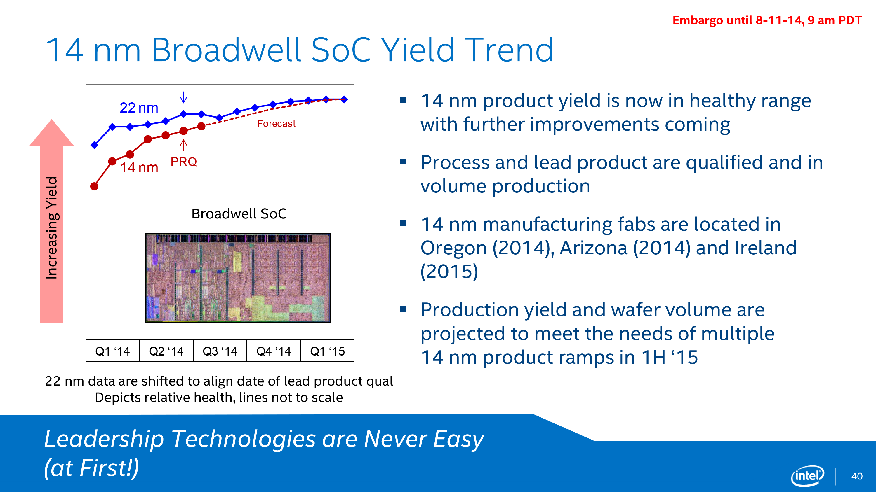
Here is a more up to date graph of Intel's 14nm yield than the one shown on page 1: http://www.fudzilla.com/images/stories/2016/Januar...As you can see, Intel didn't meet its forecast of the AnandTech graph. They were quite close in H2'14, but then the yield learning slowed down considerably. In the image of AT, they forecasted parity in H1'15, but in their latest graph (mine is from november '15), they forecasted mid-2016 for yield parity compared to 22nm. My guess from what I've heard from them is that this is fairly accurate. Yields should be pretty healthy by now.
lilmoe - Tuesday, August 30, 2016 - link
Ridiculous MSRPs as usual.rahvin - Tuesday, August 30, 2016 - link
As always, but I would consider the lack of built-in USB 3.1 a stunning failure. KL was under design when the 3.1 standard was finalized. Mark my words, but this time next year every single phone tablet is going to be using Type-C. Though you can use the port without the 3.1 spec it's a stunning failure on Intel's part to not integrate it when they are a key member of the USB forum.Personally I think they are doing it because they try to push people to thunderbird but it makes their default product a failure that needs another chip to provide what will be default functionality in 12 months.
beginner99 - Wednesday, August 31, 2016 - link
USB-C and USB 3.1 are not the same thing. You can use C-connector with USB 3.0 or old connector with USB 3.1doggface - Wednesday, August 31, 2016 - link
They could have supported USB3.1, but it is a bandwidth hungry monster that takes up die space. Instead they support pcie3x4 and oems can get/pay for the extra USB3.1 chip out of their own moneys. USB-c on the other hand can be hung of pretty much anything because it is just a connector.someonesomewherelse - Thursday, September 1, 2016 - link
The only way you can expect lower prices/better chips on desktop (i3 becoming 4c/8t, i5 8c/16t, i7 12c/24t and the no gpu chip with extra cores/cache desired by pc enthusiasts (lets name it i8 and give it 18c/36t and as much extra l3 cache you can fit on it with the space gained by the removal of the gpu... you could even have i6 (14c/28t) and i4 (6c/12t) chips using the same chips with defects on some of the cores/l3 and an i2 with 3c/6t or 4c/8t but with an extremely high clock rate (5GHz+ base)), no more random removal of some instructions (K class missing some of the virtualization for example), a turbo only limited by actual heat and power, mandatory ecc, 4 channel memory (which means that the high end now gets 8 channels), extra pcie lanes, unlocked multipliers and so on) is if Zen is actually faster than AMD marketing claims.So if you are a religious person start praying....
someonesomewherelse - Thursday, September 1, 2016 - link
Obviously at the same/lower price as current i3/i5/i7 chips.