Intel Announces 7th Gen Kaby Lake: 14nm PLUS, Six Notebook SKUs, Desktop coming in January
by Ganesh T S & Ian Cutress on August 30, 2016 9:00 AM EST- Posted in
- CPUs
- Intel
- 14nm
- Kaby Lake
- Gen 9
- Speed Shift
- Turbo Boost
When Intel first announced the shift from the dual-stage ‘Tick-Tock’ methodology that had driven their core CPU design teams for over a decade into the three-way ‘Process, Architecture, Optimization’ paradigm, there were questions as to how much of the final stage, the Optimization, would actually change the way CPUs were presented or offer upgrades in performance. At the time, ‘Kaby Lake’ as the name for Intel’s third crack at their 14nm process was well known, but users wondered if it was just another Devil’s Canyon (better overclocking) or a full on CPU launch. Well the answer is the latter, and the launch is staggered between today and January. Roll on Kaby Lake. Is that Kah-bee Lake, or Kay-bee Lake?
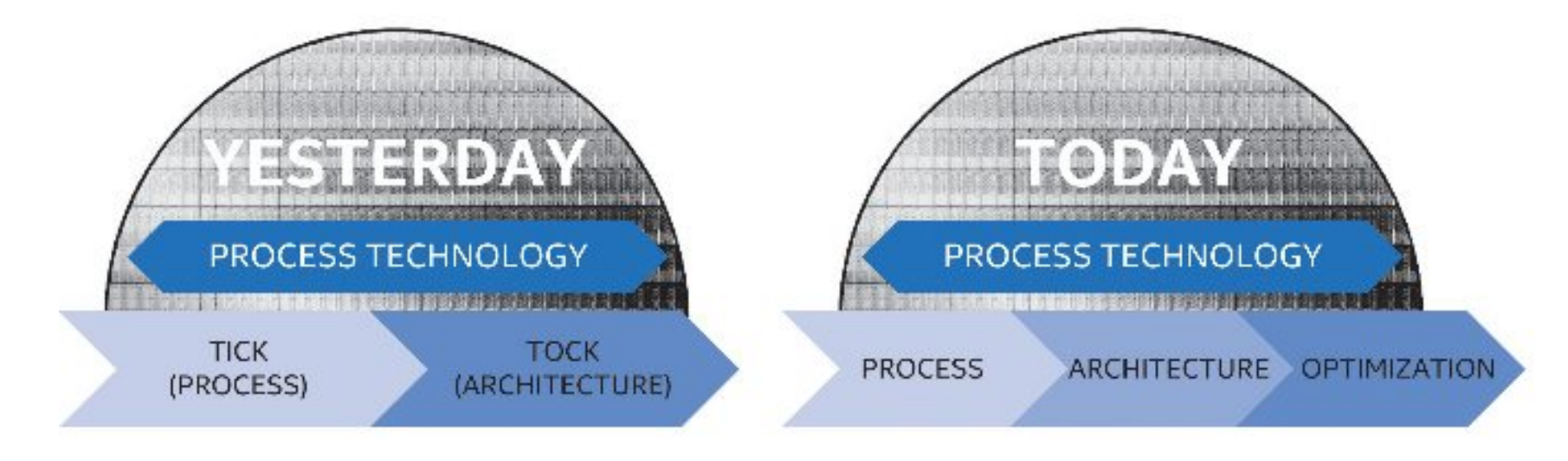
Tick-Tock to Process-Architecture-Optimization (PAO)
Intel’s two year processor cadence of Tick-Tock allowed the company to alternate reducing the lithography node (a tick) with an upgraded microarchitecture (a tock) with modest gains of performance. Each stage of the Tick-Tock would take 12-15 months, with new lithography nodes taking longer and longer to reach maturity. Eventually it has gotten to a point where 14nm took too long to become pervasive in Intel’s product stack. For a manufacturing company and a CPU company, slowly rolling out Broadwell notebook and low power parts and then gutting the mid-range desktop was the result of the troubles of bringing 14nm to the prime time. Now in 2016 we have the launch of full-sized Broadwell-EP server parts running up to 22 cores in a 145W envelope, but the low power parts are a couple of microarchitectures ahead. We have this strange situation of a stretched landscape, partially driven by markets but also for manufacturing.
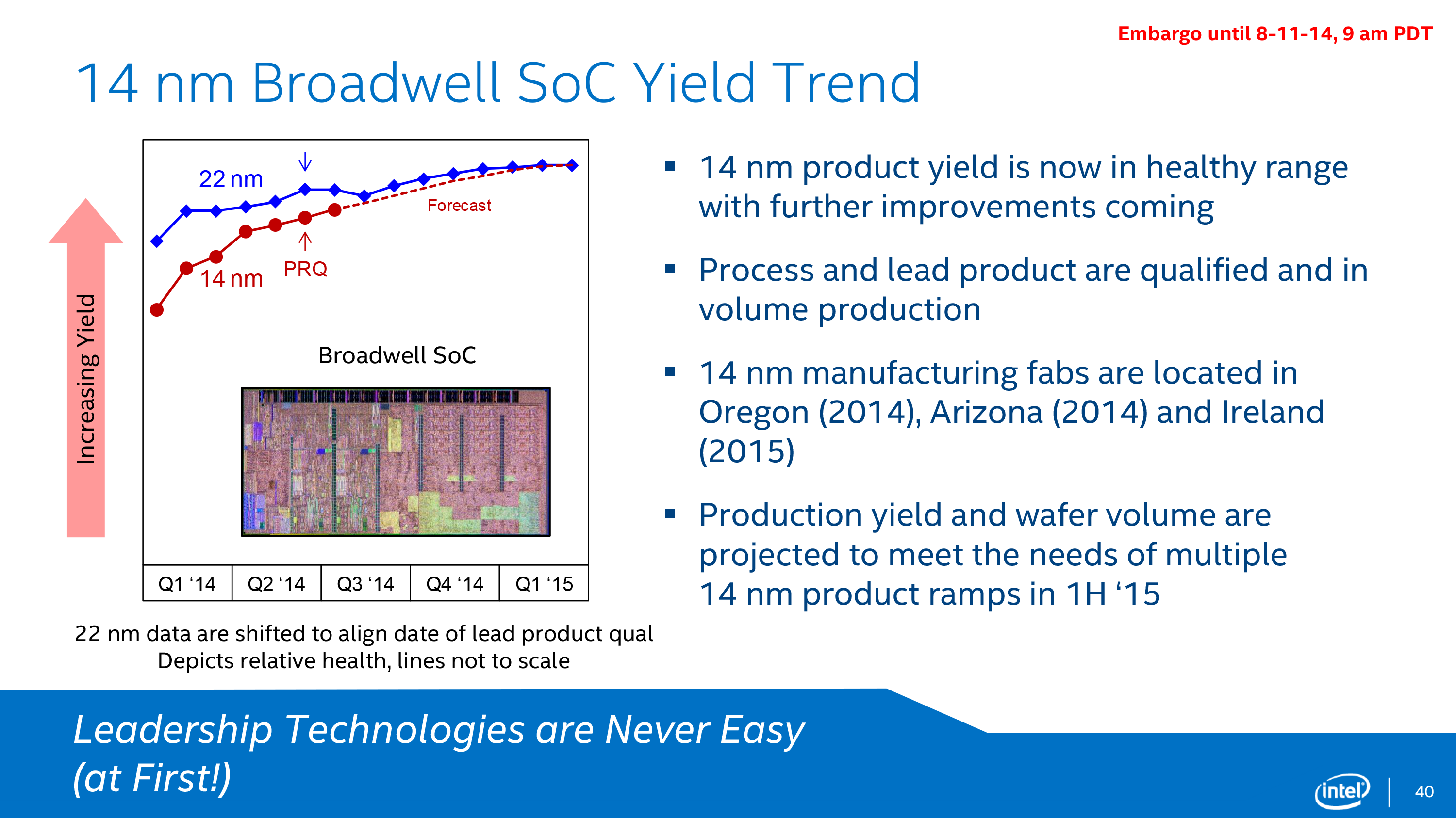
The move from Intel’s 14nm process to 10nm is a long, slow burn, taking much longer to develop than any process previous. We first saw 14nm in Broadwell mobile CPUs in Q3 of 2014, almost two years ago, and 10nm still isn’t on any public roadmap for early 2017. With the tick-tock strategy, and the launch of Skylake in mid-2015, this would leave Intel without a new CPU launch for almost two years, which is unheard of from Intel. Also, Intel’s partners rely on product cycles to announce and launch new products to generate revenue. To fill the gap, plus with a few other techniques, Intel moved to Process-Architecture-Optimization, or PAO for short.
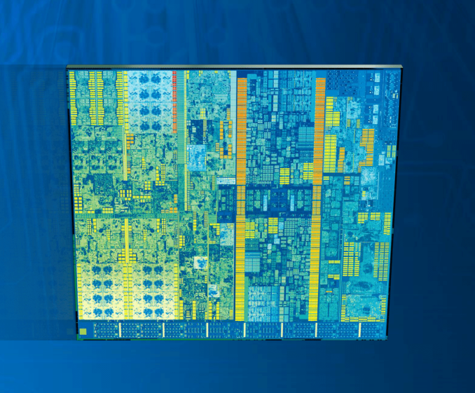
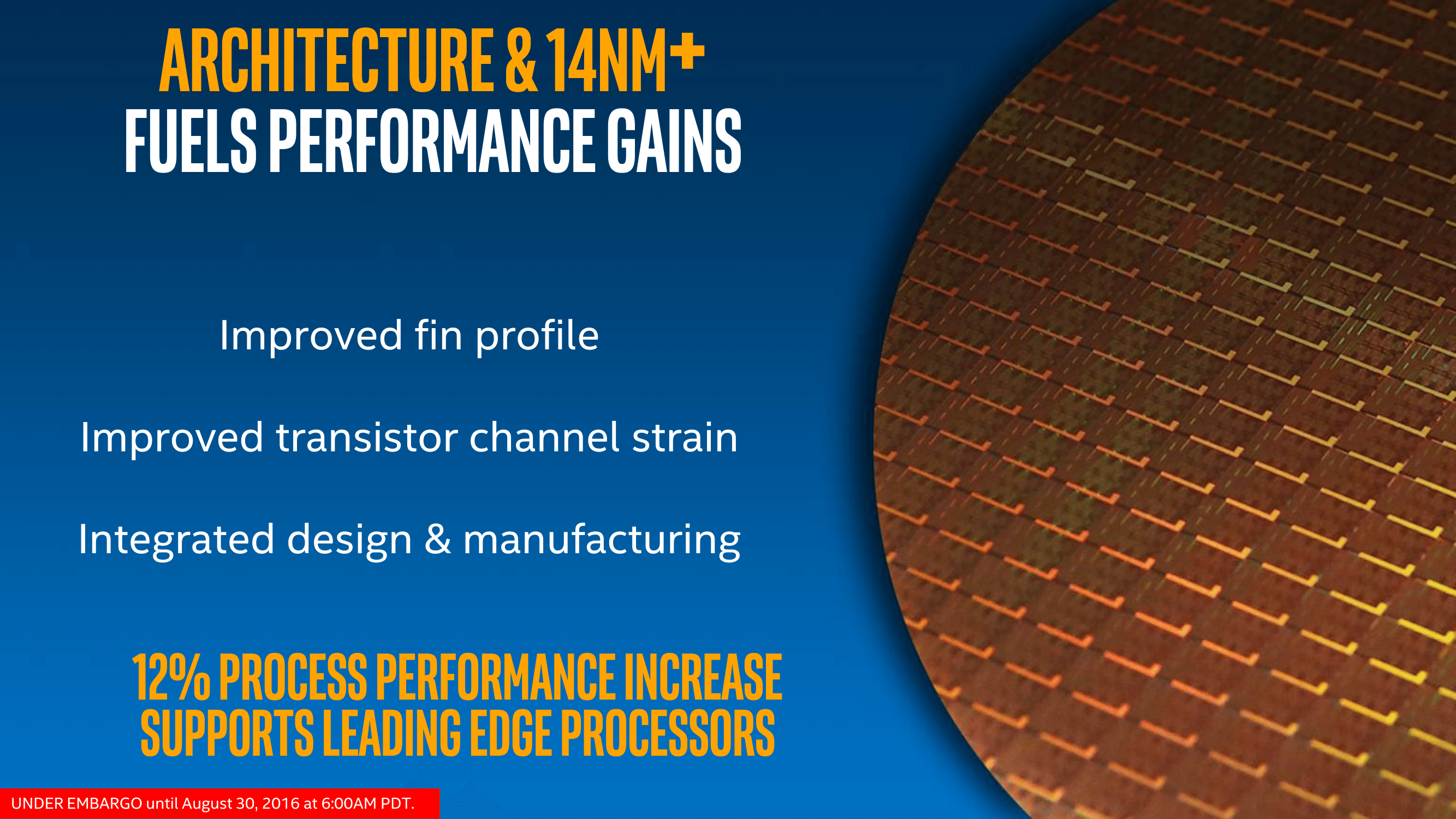
This means three bites of the cherry for 14nm before we see 10nm in prime time. First it was Broadwell, then Skylake, and today Intel is announcing Kaby Lake. As part of the release, Intel has mentioned that a number of key benefits for Kaby Lake will be based on an optimized 14nm process, called 14PLUS (or 14nm+, 14FF+). This process as a quick summary has a higher fin height and larger pitch, essentially giving a less-dense set of transistors that have more room to breathe. Normally a larger pitch means more voltage required, but this is offset by the fin height and Intel says is good for another few hundred MHz for performance. The less-dense design, in theory, may also help in overclocking, however we will have to wait until January to see those results.
Today’s Announcement
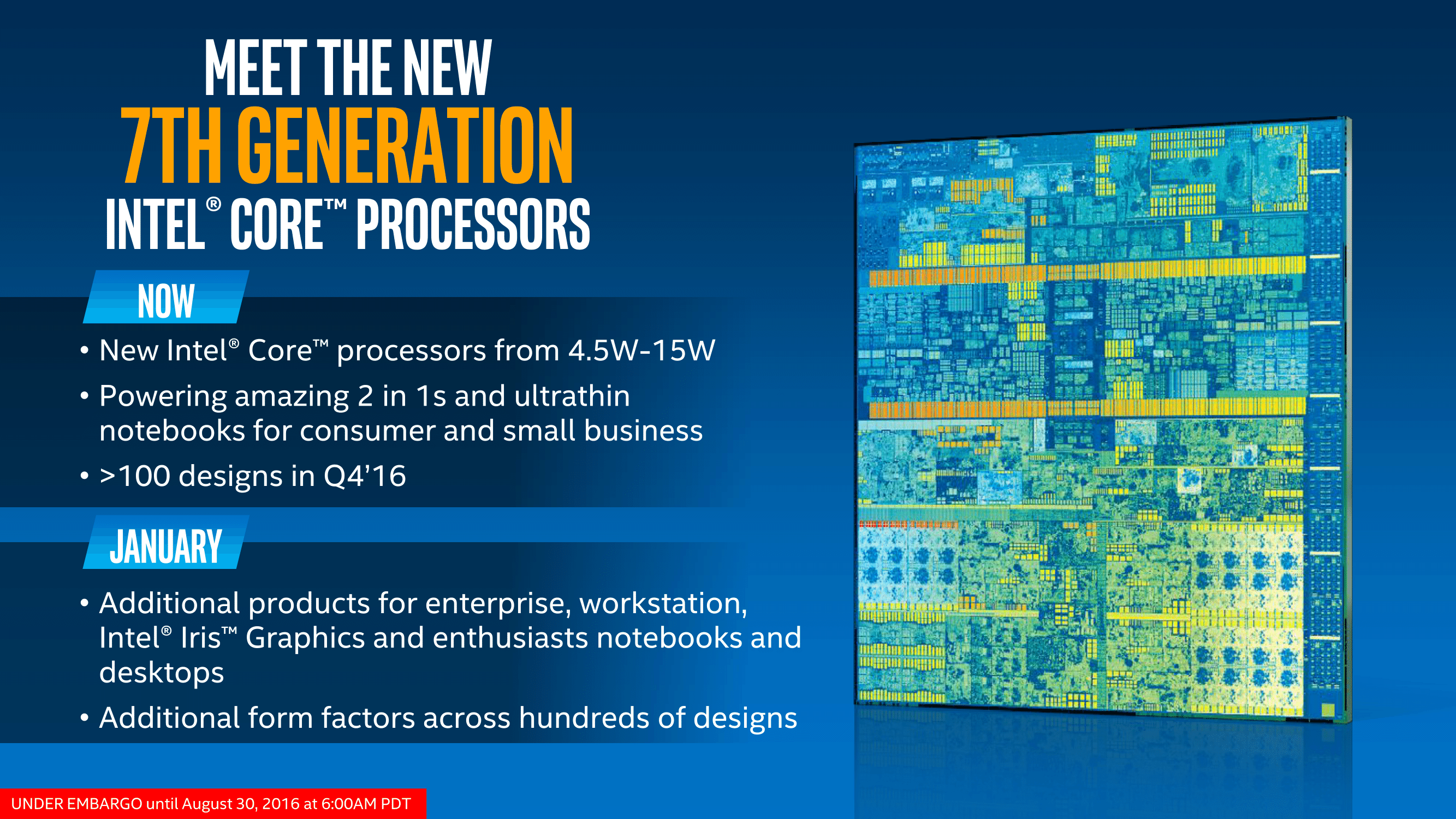
The reveal today covers several aspects of Kaby Lake. First is the actual SKUs that will be launched, which consist of three Kaby Lake-Y parts around 4.5W aimed at high-end tablets and 2-in-1 devices and three Kaby Lake-U parts at 15W for notebooks. Both sets of KBL-Y and KBL-U CPUs will feature in mini-PCs as well, so we expect to see the usual array of Zotac and ECS announcements in due course. We have details on all six CPUs to give you, including the new Core M branding regime for the 4.5W family of parts.
The pre-briefings we have had go into some detail regarding changes in the processor, particularly regarding the new enhanced media blocks inside the GPU to support new encode/decode features. The graphics power, in terms of EUs or the microarchitecture, hasn’t changed but the fixed function hardware has some nice upgrades for an updated version of Gen 9 graphics aimed at the upcoming era of 4K support. Ganesh has gone into detail for us over what that means, especially where power and battery life is concerned for anyone creating/consuming 4K content.
Kaby Lake also has an updated Speed Shift package, to accelerate the work already done with Skylake in boosting the performance of the CPU quicker to save power. Intel call it a refinement in the mechanism of handing frequency control back from the OS to the CPU, however ‘Speed Shift v2’ is an adequate moniker to show the upgraded difference.
Intel hasn’t gone into much detail regarding the new 14nm+ process itself in terms of specifics, but has listed a number of performance gains that come out of the new CPU. The fundamental microarchitecture between Skylake and the new Kaby Lake parts is practically unchanged (DMI 3.0 now allows PCIe 3.0 x4 NVMe drives from the integrated PCH), but the updated fin profile and reduced ‘strain’ by the larger fin pitch is being quoted as giving a 12% performance increase due to process alone, typically through additional frequency for the same power. The main benefits to KBL will be in that frequency due to the 14nm+ process as well as the new media capabilities.
As always, Intel consistently emphasizes the difference between a new notebook/2-in-1 based on a 15W Kaby Lake processor compared to a 5-year old device, such one based on a mobile Sandy Bridge ULV part. Intel continually sees its market revolving around new experiences created by new form factors, and to generate revenue requires people to upgrade and decide how these new experiences can influence an upgrade. Intel expects to have over 100 Kaby Lake system designs in the consumer channel by Q4, including 120+ using Thunderbolt 3, 100+ using Windows Hello (either via a Real Sense camera or a fingerprint sensor), 50+ designs with 4K UHD as a primary feature and 25+ designs with contact enabled pens. Kaby Lake should be pin compatible with Skylake based designs, meaning that for a number of cases we will simply see a drop in, but others will have new design IDs on show.


129 Comments
View All Comments
rhysiam - Tuesday, August 30, 2016 - link
They speculate on page 4 whether some retooling is required for the new 14nm+ process, and therefore whether perhaps only one or two fabs are going to be up and running early. If Intel has limited output it makes sense to direct early production to the valuable CPUs per mm2 of wafer... which is precisely these standard U and Y series processors (maybe some Xeon CPUs are higher earners, but the platform isn't ready yet). Mobile Iris Pro CPUs and most desktop processors require much more die area... meaning less output.All speculation at this point, but it is a possible answer to your question.
TEAMSWITCHER - Tuesday, August 30, 2016 - link
Ok, that makes sense. I always thought they were the same chips - with the Iris Pro features disabled. But if they are smaller dies then the bottom up approach could help to perfect the process before switching to the larger dies - potentially reducing the number of defective chips. Thanks.A5 - Tuesday, August 30, 2016 - link
It's yield and profit concerns. Doing the big chips first means they have to throw more of them away, which cuts down their profits.bryanlarsen - Tuesday, August 30, 2016 - link
Smaller chips yield dramatically better when defects are high. Imagine a die that holds 100 large chips and there are 100 defects on the die. Some of the chips will have more than one defect so there will be a few chips that are good, perhaps 15-25 or so. Now imagine that you are putting 200 smaller chips on the same die with 100 defects. You'll get at least 100 good chips, perhaps 110-120. So unless you can sell the large chip for 6-8x the cost of the small chip, it's more profitable to start with the small chips when defect rates are high.retrospooty - Tuesday, August 30, 2016 - link
The answer to almost any question like that is - they think it will be more profitable for them. They arent just thinking about the latest fastest thing, they are thinking about production, orders, volume and stock levels.quadrivial - Tuesday, August 30, 2016 - link
The answer is most likely ARM.Intel has zero competition in the high-end CPU front. People who can't wait will pay just as much for last-gen chips because that's all that's on the market. People who can wait won't mind a few months (and don't really have an option). In contrast, Intel lives in fear of Qualcomm, Samsung, or AMD announcing an ARM chip competitive with x86. Taking a more aggressive stance and coming to market as soon as possible is what Intel shareholders will want to see.
CaedenV - Tuesday, August 30, 2016 - link
True story. I can cry all I want about wanting a faster desktop chip, but the simple fact of the matter is that I will be forced to wait for Intel to release one because I am not tempted to move to AMD any time soon.But that the same time there are hundreds of schools debating between ARM and Intel chromebooks and chromeboxes, and whoever offers the lowest price is going to win the day. Releasing the smaller cheaper chips ASAP will prevent loosing those sales to ARM.
doggface - Wednesday, August 31, 2016 - link
Only problem with your theory is these chips are priced at well above the cost of a Chromebook processor. We are talking $2-400 for these chips. Arm processors can be less than $50. Not even the same league.Intel has ceded the low end of the market to Arm with the discontinuation of atom.
fanofanand - Wednesday, August 31, 2016 - link
Intel charges more for the chip than most chromebooks cost.Meteor2 - Wednesday, August 31, 2016 - link
None of this stuff (KBL) competes with ARM, it's aimed squarely at Apple. Broxton is the ARM competitor.